
QDRTM-II+ SRAM 4-Word Burst Architecture (2.0 Cycle Read Latency) Specification Sheet
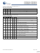
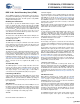
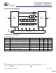
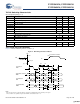
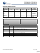
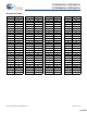
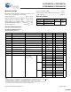
Table Of Contents
- Features
- Configurations
- Functional Description
- Selection Guide
- Logic Block Diagram (CY7C1541V18)
- Logic Block Diagram (CY7C1556V18)
- Logic Block Diagram (CY7C1543V18)
- Logic Block Diagram (CY7C1545V18)
- Pin Configuration
- Pin Definitions
- Functional Overview
- Application Example
- Write Cycle Descriptions
- Write Cycle Descriptions
- Write Cycle Descriptions
- IEEE 1149.1 Serial Boundary Scan (JTAG)
- TAP Controller State Diagram
- TAP Controller Block Diagram
- TAP Electrical Characteristics
- TAP AC Switching Characteristics
- TAP Timing and Test Conditions
- Identification Register Definitions
- Scan Register Sizes
- Instruction Codes
- Boundary Scan Order
- Power Up Sequence in QDR-II+ SRAM
- Maximum Ratings
- Operating Range
- Electrical Characteristics
- Capacitance
- Thermal Resistance
- Switching Characteristics
- Switching Waveforms
- Ordering Information
- Package Diagram
- Document History Page

CY7C1541V18, CY7C1556V18
CY7C1543V18, CY7C1545V18
Document Number: 001-05389 Rev. *F Page 11 of 28
The write cycle description table for CY7C1556V18 follows.
[3, 11]
Write Cycle Descriptions
BWS
0
K K
L L–H – During the Data portion of a write sequence, the single byte (D
[8:0]
) is written into the device.
L – L–H During the Data portion of a write sequence, the single byte (D
[8:0]
) is written into the device.
H L–H – No data is written into the device during this portion of a write operation.
H – L–H No data is written into the device during this portion of a write operation.
The write cycle description table for CY7C1545V18 follows.
[3, 11]
Write Cycle Descriptions
BWS
0
BWS
1
BWS
2
BWS
3
K K Comments
LLLLL–H–During the Data portion of a write sequence, all four bytes (D
[35:0]
) are written into
the device.
LLLL–L–HDuring the Data portion of a write sequence, all four bytes (D
[35:0]
) are written into
the device.
L H H H L–H – During the Data portion of a write sequence, only the lower byte (D
[8:0]
) is written
into the device. D
[35:9]
remains unaltered.
L H H H – L–H During the Data portion of a write sequence, only the lower byte (D
[8:0]
) is written
into the device. D
[35:9]
remains unaltered.
H L H H L–H – During the Data portion of a write sequence, only the byte (D
[17:9]
) is written into
the device. D
[8:0]
and D
[35:18]
remains unaltered.
H L H H – L–H During the Data portion of a write sequence, only the byte (D
[17:9]
) is written into
the device. D
[8:0]
and D
[35:18]
remains unaltered.
H H L H L–H – During the Data portion of a write sequence, only the byte (D
[26:18]
) is written into
the device. D
[17:0]
and D
[35:27]
remains unaltered.
H H L H – L–H During the Data portion of a write sequence, only the byte (D
[26:18]
) is written into
the device. D
[17:0]
and D
[35:27]
remains unaltered.
H H H L L–H – During the Data portion of a write sequence, only the byte (D
[35:27]
) is written into
the device. D
[26:0]
remains unaltered.
H H H L – L–H During the Data portion of a write sequence, only the byte (D
[35:27]
) is written into
the device. D
[26:0]
remains unaltered.
HHHHL–H–No data is written into the device during this portion of a write operation.
HHHH–L–HNo data is written into the device during this portion of a write operation.
[+] Feedback [+] Feedback