
Dual-Port Static RAM with SEM, INT, BUSY Specification Sheet
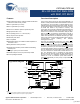


CY7C145, CY7C144
Document #: 38-06034 Rev. *D Page 3 of 21
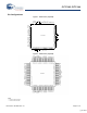
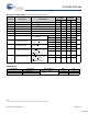
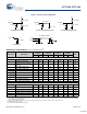
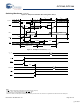
Figure 3. 80-Pin TQFP
Pin Configurations (continued)
1
2
3
4
5
6
7
8
9
10
11
12
13
14
15
17
16
18
19
20
21
22
23
24
25
26
27
28
29
30
31
32
33
34
35
37
36
38
39
40
60
59
58
57
56
55
54
53
52
51
50
49
48
47
46
44
45
43
42
41
80
79
78
77
76
75
74
73
72
71
70
69
68
67
66
64
65
63
62
61
/O
2L
/O
3L
/O
4L
/O
5L
/O
6L
/O
7L
V
CC
GND
/O
0R
/O
1R
2R
/O
3R
/O
4R
5R
GND
V
CC
V
CC
OE
L
I/O
0L
I/O
8L
A
5L
A
12L
A
11L
A
10L
A
9L
A
8L
A
7L
A
6L
CE
L
SEM
L
R/W
L
A
4L
A
3L
A
2L
A
1L
A
0L
GND
BUSY
L
M/S
A
0R
A
1R
A
2R
A
3R
A
4R
INT
L
GND
OE
R
/O
6R
A
12R
A
11R
A
10R
A
9R
A
8R
A
7R
A
6R
NC
CE
R
SEM
R
R/W
R
CY7C145
BUSY
R
INT
R
I/O
8R
NC
NC
NC
NC
NC
NC
NC
NC
NC
NC
NC
NC
NC
A
5R
I/O
7R
NC
/O
O
NC
I/O
1L
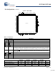
Table 1. Pin Definitions
Left Port Right Port Description
I/O
0L−7L(8L)
I/O
0R−7R(8R)
Data bus Input/Output
A
0L−12L
A
0R−12R
Address Lines
CE
L
CE
R
Chip Enable
OE
L
OE
R
Output Enable
R/W
L
R/W
R
Read/Write Enable
SEM
L
SEM
R
Semaphore Enable. When asserted LOW, allows access to eight semaphores. The three least signif-
icant bits of the address lines will determine which semaphore to write or read. The I/O
0
pin is used
when writing to a semaphore. Semaphores are requested by writing a 0 into the respective location.
INT
L
INT
R
Interrupt Flag. INT
L
is set when right port writes location 1FFE and is cleared when left port reads
location 1FFE. INT
R
is set when left port writes location 1FFF and is cleared when right port reads
location 1FFF.
BUSY
L
BUSY
R
Busy Flag
M/S
Master or Slave Select
V
CC
Power
GND Ground
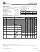
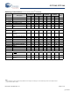
Table 2. Selection Guide
Description
7C144-15
7C145-15
7C144-25
7C145-25
7C144-35
7C145-35
7C144-55
7C145-55
Unit
Maximum Access Time 15 25 35 55 ns
Maximum Operating Current 220 180 160 160 mA
Maximum Standby Current for I
SB1
60 40 30 30 mA
[+] Feedback