CY7C1380C CY7C1382C 18-Mb (512K x 36/1M x 18) Pipelined SRAM Functional Description[1] Features • Supports bus operation up to 250 MHz • Available speed grades are 250, 225, 200,166 and 133MHz • Registered inputs and outputs for pipelined operation • 3.3V core power supply • 2.5V / 3.3V I/O operation • Fast clock-to-output times — 2.6 ns (for 250-MHz device) — 2.8 ns (for 225-MHz device) — 3.0 ns (for 200-MHz device) — 3.4 ns (for 166-MHz device) — 4.
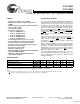
CY7C1380C CY7C1382C 1 Logic Block Diagram – CY7C1380C (512K x 36) A0, A1, A ADDRESS REGISTER 2 A[1:0] MODE ADV CLK Q1 BURST COUNTER CLR AND Q0 LOGIC ADSC ADSP BWD DQD ,DQPD BYTE WRITE REGISTER DQD ,DQPD BYTE WRITE DRIVER BWC DQC ,DQPC BYTE WRITE REGISTER DQC ,DQPC BYTE WRITE DRIVER DQB ,DQPB BYTE WRITE REGISTER DQB ,DQPB BYTE WRITE DRIVER BWB BWA BWE GW CE1 CE2 CE3 OE ZZ SENSE AMPS OUTPUT REGISTERS OUTPUT BUFFERS E DQs DQPA DQPB DQPC DQPD DQA ,DQPA BYTE WRITE DRIVER DQA ,DQPA BYTE W
CY7C1380C CY7C1382C Pin Configurations NC NC NC VDDQ VSSQ NC NC DQB DQB VSSQ VDDQ DQB DQB NC VDD NC VSS DQB DQB VDDQ VSSQ DQB DQB DQPB NC VSSQ VDDQ NC NC NC 1 2 3 4 5 6 7 8 9 10 11 12 13 14 15 16 17 18 19 20 21 22 23 24 25 26 27 28 29 30 CY7C1382C (1M x 18) 80 79 78 77 76 75 74 73 72 71 70 69 68 67 66 65 64 63 62 61 60 59 58 57 56 55 54 53 52 51 Document #: 38-05237 Rev.
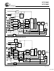
CY7C1380C CY7C1382C Pin Configurations (continued) 119-ball BGA (1 Chip Enable with JTAG) 1 CY7C1380C (512K x 36) 3 4 5 A A ADSP A VDDQ 2 A B C NC NC A A A A ADSC VDD A A A A NC NC D E DQC DQC DQPC DQC VSS VSS NC CE1 VSS VSS DQPB DQB DQB DQB F VDDQ DQC VSS OE VSS DQB VDDQ G H J K DQC DQC VDDQ DQD DQC DQC VDD DQD BWC VSS NC VSS ADV BWB VSS NC VSS DQB DQB VDD DQA DQB DQB VDDQ DQA BWA VSS DQA DQA DQA VDDQ VSS DQA DQA GW VDD CLK NC 6 A 7 VDDQ L DQD DQD M VDDQ
CY7C1380C CY7C1382C Pin Configurations (continued) 165-ball fBGA CY7C1380C (512K x 36) 1 A B C D E F G H J K L M N P NC / 288M R 2 A 3 4 5 6 7 8 9 10 11 CE1 BWC BWB CE3 BWE ADSC ADV A NC NC A CE2 BWD BWA CLK GW A NC / 144M NC DQC VDDQ VSS VSS VSS VSS VSS VSS VDDQ VDDQ VSS VDD OE VSS VDD ADSP DQPC DQC VDDQ NC DQB DQPB DQB DQC DQC VDDQ VDD VSS VSS VSS VDD VDDQ DQB DQB DQC DQC NC DQD DQC VDDQ VDD VSS VSS VSS VDD DQB DQB DQC VSS DQD VDDQ NC VDD
CY7C1380C CY7C1382C CY7C1380C–Pin Definitions Name TQFP BGA fBGA I/O Description R6,P6,A2, InputAddress Inputs used to select one of the P4,N4, A10,B2, Synchronous 256K address locations. Sampled at the rising A2,B2, B10,N6,P3,P4, edge of the CLK if ADSP or ADSC is active C2,R2, P8,P9,P10, LOW, and CE1, CE2, and CE3 [2]are sampled A3,B3,C3, T3,T4,A5,B5, P11,R3,R4,R8, active. A1: A0 are fed to the two-bit counter..
CY7C1380C CY7C1382C CY7C1380C–Pin Definitions (continued) Name TQFP BGA fBGA 84 A4 B9 InputAddress Strobe from Processor, sampled Synchronous on the rising edge of CLK, active LOW. When asserted LOW, addresses presented to the device are captured in the address registers. A1: A0 are also loaded into the burst counter. When ADSP and ADSC are both asserted, only ADSP is recognized. ASDP is ignored when CE1 is deasserted HIGH.
CY7C1380C CY7C1382C CY7C1380C–Pin Definitions (continued) Name TQFP BGA fBGA I/O VSSQ 5,10,21,26,55, 60,71, 76 - - I/O Ground Ground for the I/O circuitry. VDDQ 4,11,20,27,54, A1,F1,J1,M1, C3,C9,D3,D9, 61,70, U1, E3,E9,F3,F9,G 77 A7,F7,J7,M7, 3, U7 G9,J3,J9, K3,K9,L3, L9,M3,M9,N3, N9 I/O Power Supply Power supply for the I/O circuitry. MODE 31 R3 R1 TDO - U5 P7 TDI - U3 P5 JTAG serial Serial data-In to the JTAG circuit. Sampled input on the rising edge of TCK.
CY7C1380C CY7C1382C CY7C1382C:Pin Definitions Name TQFP BGA A0, A1 , A 37,36,32, 33,34,35, 42,43,44, 45,46,47, 48,49,50, 80,81,82, 99,100 P4,N4, A2,B2, C2,R2, T2,A3, B3,C3, T3,A5, B5,C5, T5,A6, B6,C6, R6,T6 BWA,BWB 93,94 G3,L5 B5,A4 InputByte Write Select Inputs, active LOW. Qualified Synchronous with BWE to conduct byte writes to the SRAM. Sampled on the rising edge of CLK. GW 88 H4 B7 InputGlobal Write Enable Input, active LOW.
CY7C1380C CY7C1382C CY7C1382C:Pin Definitions (continued) Name TQFP BGA fBGA 84 A4 B9 InputAddress Strobe from Processor, sampled on Synchronous the rising edge of CLK, active LOW. When asserted LOW, addresses presented to the device are captured in the address registers. A1: A0 are also loaded into the burst counter. When ADSP and ADSC are both asserted, only ADSP is recognized. ASDP is ignored when CE1 is deasserted HIGH.
CY7C1380C CY7C1382C CY7C1382C:Pin Definitions (continued) Name VDDQ MODE TQFP BGA 4,11,20,27,54, A1,A7,F1,F7, 61,70, J1,J7,M1,M7, 77 U1,U7 fBGA I/O Description C3,C9,D3,D9, I/O Power Sup- Power supply for the I/O circuitry. ply E3,E9, F3,F9,G3, G9,J3,J9, K3,K9,L3, L9,M3,M9,N3, N9 31 R3 R1 TDO - U5 P7 TDI - U3 P5 JTAG serial Serial data-In to the JTAG circuit. Sampled on the rising edge of TCK.
CY7C1380C CY7C1382C Functional Overview All synchronous inputs pass through input registers controlled by the rising edge of the clock. All data outputs pass through output registers controlled by the rising edge of the clock. Maximum access delay from the clock rise (tCO) is 3.0ns (200-MHz device). The CY7C1380C supports secondary cache in systems utilizing either a linear or interleaved burst sequence. The interleaved burst order supports Pentium and i486™ processors.
CY7C1380C CY7C1382C Asserting ADV LOW at clock rise will automatically increment the burst counter to the next address in the burst sequence. Both Read and Write burst operations are supported. Sleep Mode The ZZ input pin is an asynchronous input. Asserting ZZ places the SRAM in a power conservation “sleep” mode. Two clock cycles are required to enter into or exit from this “sleep” mode. While in this mode, data integrity is guaranteed.
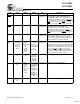
CY7C1380C CY7C1382C Truth Table[ 3, 4, 5, 6, 7, 8] Operation Add.
CY7C1380C CY7C1382C IEEE 1149.1 Serial Boundary Scan (JTAG) Test MODE SELECT (TMS) The CY7C1380C incorporates a serial boundary scan test access port (TAP). This port operates in accordance with IEEE Standard 1149.1-1990 but does not have the set of functions required for full 1149.1 compliance. These functions from the IEEE specification are excluded because their inclusion places an added delay in the critical speed path of the SRAM.
CY7C1380C CY7C1382C TDI and TDO balls as shown in the Tap Controller Block Diagram. Upon power-up, the instruction register is loaded with the IDCODE instruction. It is also loaded with the IDCODE instruction if the controller is placed in a reset state as described in the previous section. When the TAP controller is in the Capture-IR state, the two least significant bits are loaded with a binary “01” pattern to allow for fault isolation of the board-level serial test data path.
CY7C1380C CY7C1382C Note that since the PRELOAD part of the command is not implemented, putting the TAP to the Update-DR state while performing a SAMPLE/PRELOAD instruction will have the same effect as the Pause-DR command. register is placed between the TDI and TDO balls. The advantage of the BYPASS instruction is that it shortens the boundary scan path when multiple devices are connected together on a board.
CY7C1380C CY7C1382C 3.3V TAP AC Test Conditions 2.5V TAP AC Test Conditions Input pulse levels ........ ........................................VSS to 3.3V Input pulse levels...............................................VSS to 2.5V Input rise and fall times ...................... ..............................1ns Input rise and fall time ......................................................1ns Input timing reference levels ...........................................1.
CY7C1380C CY7C1382C Identification Register Definitions CY7C1380C (512KX36) CY7C1382C (1MX18) 010 0100 Describes the version number.
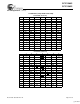
CY7C1380C CY7C1382C 119-Ball BGA Boundary Scan Order CY7C1380C (512K x 36) BIT# BALL ID BIT# BALL ID 1 K4 37 B2 2 H4 38 P4 3 M4 39 N4 4 F4 40 R6 5 B4 41 T5 6 A4 42 T3 7 G4 43 R2 8 C6 44 R3 9 A6 45 P2 10 D6 46 P1 11 D7 47 N2 12 E6 48 L2 13 G6 49 K1 14 H7 50 N1 15 E7 51 M2 16 F6 52 L1 17 G7 53 K2 18 H6 54 Not Bonded (Preset to 1) 19 T7 55 H1 20 K7 56 G2 21 L6 57 E2 22 N6 58 D1 23 P7 59 H2 24 K6 60 G1 25 L7 6
CY7C1380C CY7C1382C 119-Ball BGA Boundary Scan Order CY7C1382C (1M x 18) BIT# BALL ID BIT# BALL ID 1 K4 37 B2 2 H4 38 P4 3 M4 39 N4 4 F4 40 R6 5 B4 41 T5 6 A4 42 T3 7 G4 43 R2 8 C6 44 R3 9 A6 45 Not Bonded (Preset to 0) 10 T6 46 Not Bonded (Preset to 0) 11 Not Bonded (Preset to 0) 47 Not Bonded (Preset to 0) 12 Not Bonded (Preset to 0) 48 Not Bonded (Preset to 0) 13 Not Bonded (Preset to 0) 49 P2 14 D6 50 N1 15 E7 51 M2 16 F6 52 L1 17 G7
CY7C1380C CY7C1382C 165-Ball fBGA Boundary Scan Order CY7C1380C (512K x 36) BIT# BALL ID BIT# BALL ID 1 B6 37 N6 2 B7 38 R6 3 A7 39 P6 4 B8 40 R4 5 A8 41 R3 6 B9 42 P4 7 A9 43 P3 8 B10 44 R1 9 A10 45 N1 10 C11 46 L2 11 E10 47 K2 12 F10 48 J2 13 G10 49 M2 14 D10 50 M1 15 D11 51 L1 16 E11 52 K1 17 F11 53 J1 18 G11 54 Internal 19 H11 55 G2 20 J10 56 F2 21 K10 57 E2 22 L10 58 D2 23 M10 59 G1 24 J11 60 F1 25 K11
CY7C1380C CY7C1382C 165-Ball fBGA Boundary Scan Order CY7C1382C (1M x 18) BIT# BALL ID BIT# BALL ID 0 B6 36 N6 1 B7 37 R6 2 A7 38 P6 3 B8 39 R4 4 A8 40 R3 5 B9 41 P4 6 A9 42 P3 7 B10 43 R1 8 A10 44 Not Bonded (Preset to 0) 9 A11 45 Not Bonded (Preset to 0) 10 Not Bonded (Preset to 0) 46 Not Bonded (Preset to 0) 11 Not Bonded (Preset to 0) 47 Not Bonded (Preset to 0) 12 Not Bonded (Preset to 0) 48 N1 13 C11 49 M1 14 D11 50 L1 15 E11 51 K1 16
CY7C1380C CY7C1382C Maximum Ratings Current into Outputs (LOW)......................................... 20 mA (Above which the useful life may be impaired. For user guidelines, not tested.) Storage Temperature ................................. –65°C to +150°C Ambient Temperature with Power Applied............................................. –55°C to +125°C Supply Voltage on VDD Relative to GND........ –0.3V to +4.6V DC Voltage Applied to Outputs in Tri-State........................................... –0.
CY7C1380C CY7C1382C Electrical Characteristics Over the Operating Range[12, 13] Parameter ISB3 Description (continued) Test Conditions Min. Max. Unit 105 mA 100 mA 95 mA Automatic CE VDD = Max, Device Deselected, or 4.0-ns cycle, 250 MHz Power-down VIN ≤ 0.3V or VIN > VDDQ – 0.3V 4.4-ns cycle, 225 MHz Current—CMOS Inputs f = fMAX = 1/tCYC 5.0-ns cycle, 200 MHz ISB4 Automatic CE Power-down Current—TTL Inputs VDD = Max, Device Deselected, VIN ≥ VIH or VIN ≤ VIL, f = 0 6.
CY7C1380C CY7C1382C AC Test Loads and Waveforms 3.3V I/O Test Load R = 317Ω 3.3V OUTPUT ALL INPUT PULSES VDD OUTPUT RL = 50Ω Z0 = 50Ω 10% 90% 10% 90% GND 5 pF R = 351Ω ≤ 1ns ≤ 1ns VL = 1.5V INCLUDING JIG AND SCOPE (a) (c) (b) 2.5V I/O Test Load R = 1667Ω 2.5V OUTPUT Z0 = 50Ω 10% R =1538Ω VL = 1.25V Document #: 38-05237 Rev.
CY7C1380C CY7C1382C Switching Characteristics Over the Operating Range[19, 20] 250 MHz Parameter tPOWER Description 225 MHz 200 MHz Min. Max [15] VDD(Typical) to the first Access 167 MHz 133 MHz Min. Max Min. Max 1 1 1 Unit 1 1 ms Clock tCYC Clock Cycle Time 4.0 4.4 5 6 7.5 ns tCH Clock HIGH 1.7 2.0 2.0 2.2 2.5 ns tCL Clock LOW 1.7 2.0 2.0 2.2 2.5 ns Output Times tCO Data Output Valid After CLK Rise tDOH Data Output Hold After CLK Rise 1.
CY7C1380C CY7C1382C Switching Waveforms Read Cycle Timing[21] t CYC CLK t CH t ADS t CL t ADH ADSP tADS tADH ADSC tAS tAH A1 ADDRESS A2 tWES A3 Burst continued with new base address tWEH GW, BWE, BWx tCES Deselect cycle tCEH CE tADVS tADVH ADV ADV suspends burst.
CY7C1380C CY7C1382C Switching Waveforms (continued) Write Cycle Timing[21, 22] t CYC CLK tCH tADS tCL tADH ADSP tADS ADSC extends burst tADH tADS tADH ADSC tAS tAH A1 ADDRESS A2 A3 Byte write signals are ignored for first cycle when ADSP initiates burst tWES tWEH BWE, BWX tWES tWEH GW tCES tCEH CE t t ADVS ADVH ADV ADV suspends burst OE tDS Data In (D) High-Z t OEHZ tDH D(A1) D(A2) D(A2 + 1) D(A2 + 1) D(A2 + 2) D(A2 + 3) D(A3) D(A3 + 1) D(A3 + 2) Data Out (Q) BURST READ S
CY7C1380C CY7C1382C Switching Waveforms (continued) Read/Write Cycle Timing[21, 23, 24] tCYC CLK tCL tCH tADS tADH tAS tAH ADSP ADSC ADDRESS A1 A2 A3 A4 A5 A6 D(A5) D(A6) tWES tWEH BWE, BWX tCES tCEH CE ADV OE tDS tCO tDH tOELZ Data In (D) High-Z tCLZ Data Out (Q) High-Z Q(A1) Back-to-Back READs tOEHZ D(A3) Q(A2) Q(A4) Single WRITE Q(A4+1) Q(A4+2) BURST READ DON’T CARE Q(A4+3) Back-to-Back WRITEs UNDEFINED Note: 23.
CY7C1380C CY7C1382C Switching Waveforms (continued) ZZ Mode Timing [25, 26] CLK t ZZ ZZ I t ZZREC t ZZI SUPPLY I DDZZ t RZZI ALL INPUTS (except ZZ) Outputs (Q) DESELECT or READ Only High-Z DON’T CARE Notes: 25. Device must be deselected when entering ZZ mode. See Cycle Descriptions table for all possible signal conditions to deselect the device. 26. DQs are in high-Z when exiting ZZ sleep mode Document #: 38-05237 Rev.
CY7C1380C CY7C1382C Ordering Information Speed (MHz) 250 225 Ordering Code CY7C1380C-250AC CY7C1382C-250AC Package Name A101 Part and Package Type 100-lead Thin Quad Flat Pack (14 x 20 x 1.4mm) CY7C1380C-250BGC CY7C1382C-250BGC BG119 119 PBGA CY7C1380C-250BZC CY7C1382C-250BZC BB165A 165 fBGA CY7C1380C-225AC A101 Operating Range Commercial 100-lead Thin Quad Flat Pack (14 x 20 x 1.
CY7C1380C CY7C1382C Package Diagrams 100-Pin Thin Plastic Quad Flatpack (14 x 20 x 1.4 mm) A101 DIMENSIONS ARE IN MILLIMETERS. 16.00±0.20 1.40±0.05 14.00±0.10 100 81 80 1 20.00±0.10 22.00±0.20 0.30±0.08 0.65 TYP. 30 12°±1° (8X) SEE DETAIL A 51 31 50 0.20 MAX. 1.60 MAX. 0° MIN. STAND-OFF 0.05 MIN. 0.15 MAX. 0.25 0.10 R 0.08 MIN. 0.20 MAX. SEATING PLANE GAUGE PLANE 0°-7° R 0.08 MIN. 0.20 MAX. 0.60±0.15 0.20 MIN. 1.00 REF. DETAIL Document #: 38-05237 Rev.
CY7C1380C CY7C1382C Package Diagrams (continued) 119-Lead PBGA (14 x 22 x 2.4 mm) BG119 51-85115-*B Document #: 38-05237 Rev.
CY7C1380C CY7C1382C Package Diagrams (continued) 165-Ball FBGA (13 x 15 x 1.2 mm) BB165A 51-85122-*C i486 is a trademark, and Intel and Pentium are registered trademarks of Intel Corporation. PowerPC is a trademark of IBM Corporation. All product and company names mentioned in this document are the trademarks of their respective holders. Document #: 38-05237 Rev.
CY7C1380C CY7C1382C Document History Page Document Title: CY7C1380C/CY7C1382C 18-Mb (512K x 36/1M x 18) Pipelined SRAM Document Number: 38-05237 REV. ECN NO. Issue Date Orig. of Change Description of Change ** 116277 08/27/02 SKX New Data Sheet *A 121540 11/21/02 DSG Updated package diagrams 51-85115 (BG119) to rev. *B and 51-85122 (BB165A) to rev.