
2-Mbit (128K x 18) Flow-Through SRAM with NoBLTM Architecture Specification Sheet
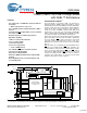

CY7C1231H
Document #: 001-00207 Rev. *B Page 7 of 12
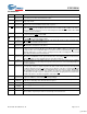
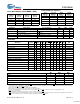
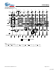
Capacitance
[11]
Parameter Description Test Conditions
100 TQFP
Max. Unit
C
IN
Input Capacitance T
A
= 25°C, f = 1 MHz,
V
DD
= 3.3V
V
DDQ
= 2.5V
5pF
C
CLOCK
Clock Input Capacitance 5 pF
C
I/O
I/O Capacitance 5 pF
Thermal Resistance
[11]
Parameters Description Test Conditions
100 TQFP
Package Unit
Θ
JA
Thermal Resistance
(Junction to Ambient)
Test conditions follow standard test methods and
procedures for measuring thermal impedance,
per EIA/JESD51
30.32 °C/W
Θ
JC
Thermal Resistance
(Junction to Case)
6.85 °C/W
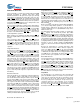
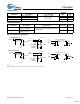
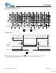
AC Test Loads and Waveforms
Note:
11. Tested initially and after any design or process change that may affect these parameters.
OUTPUT
R = 317Ω
R = 351Ω
5pF
INCLUDING
JIG AND
SCOPE
(a) (b)
OUTPUT
R
L
= 50Ω
Z
0
= 50Ω
V
L
= 1.5V
3.3V
ALL INPUT PULSES
V
DDQ
GND
90%
10%
90%
10%
≤ 1 ns
≤ 1 ns
(c)
3.3V I/O Test Load
OUTPUT
R = 1667Ω
R =1538Ω
5pF
INCLUDING
JIG AND
SCOPE
(a) (b)
OUTPUT
R
L
= 50Ω
Z
0
= 50Ω
V
T
= 1.25V
2.5V
ALL INPUT PULSES
V
DDQ
GND
90%
10%
90%
10%
≤ 1 ns
≤ 1 ns
(c)
2.5V I/O Test Load
[+] Feedback