
16-Mbit Static RAM Specification Sheet
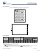
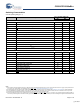
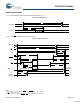
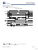
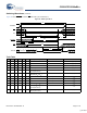
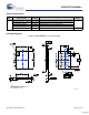
Table Of Contents
- Features
- Functional Description
- Logic Block Diagram
- Pin Configuration
- Product Portfolio
- Maximum Ratings
- Operating Range
- Electrical Characteristics
- Capacitance
- Thermal Resistance
- Data Retention Characteristics
- Switching Characteristics
- Switching Waveforms
- Truth Table
- Ordering Information
- Package Diagrams
- Document History Page
- Sales, Solutions, and Legal Information
CY62167EV30 MoBL
®
Document #: 38-05446 Rev. *E Page 7 of 14
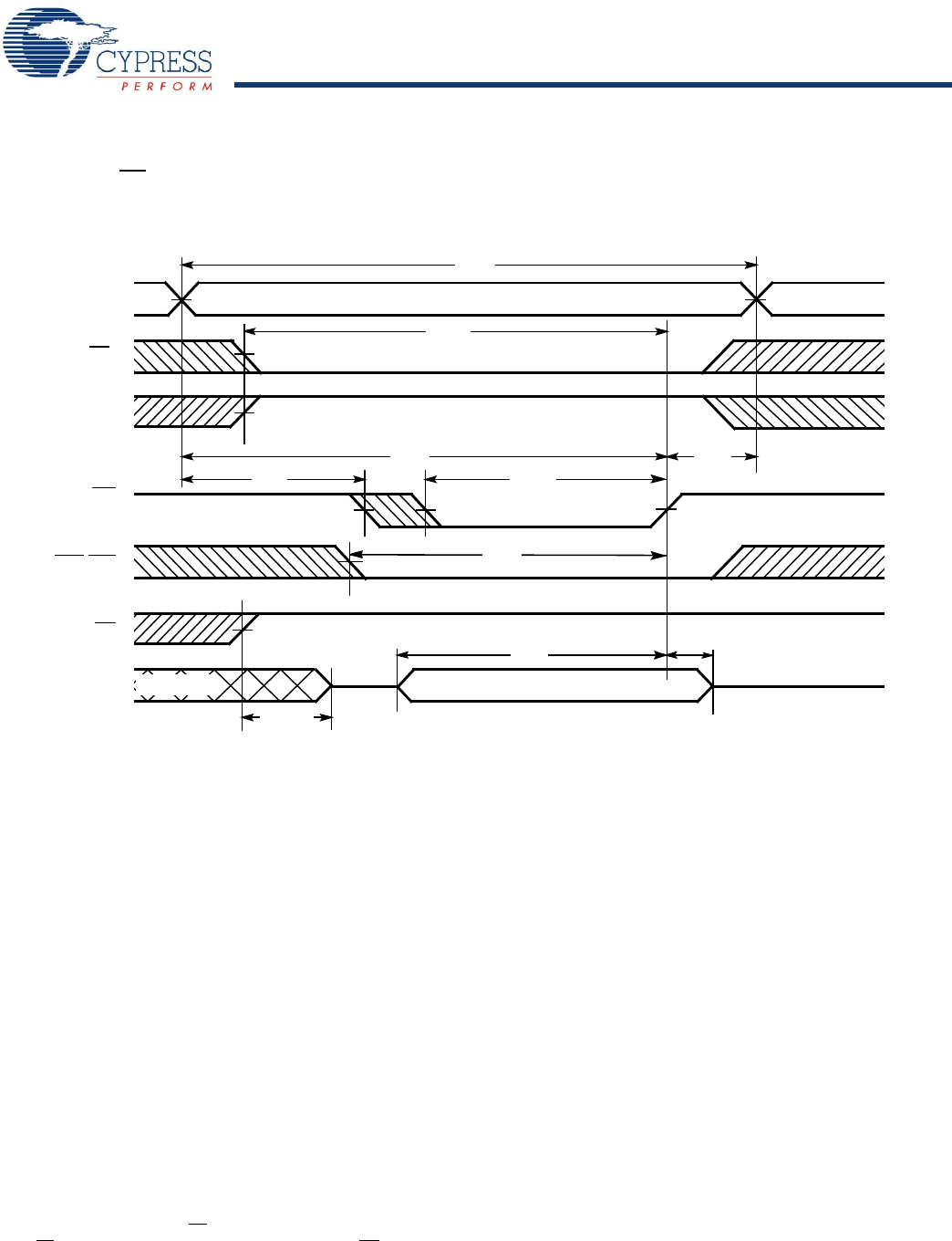
Figure 7 shows WE
controlled write cycle waveforms.
[18, 22, 23]
Figure 7. Write Cycle No. 1
Switching Waveforms (continued)
t
HD
t
SD
t
PWE
t
SA
t
HA
t
AW
t
SCE
t
WC
t
HZOE
VALID DATA
t
BW
NOTE 24
CE
1
ADDRESS
CE
2
WE
DATA I/O
OE
BHE/BLE
Notes
22. Data IO is high impedance if OE
= V
IH
.
23. If CE
1
goes HIGH and CE
2
goes LOW simultaneously with WE = V
IH
, the output remains in a high impedance state.
24. During this period the I/Os are in output state. Do not apply input signals.
[+] Feedback