
Specifications


CY14B101P
Document Number: 001-44109 Rev. *O Page 28 of 36
AutoStore or Power-Up RECALL
Over the Operating Range
Parameter Description
CY14B101P
Unit
Min Max
t
FA
[19]
Power-Up RECALL duration – 20 ms
t
STORE
[20]
STORE cycle duration – 8 ms
t
DELAY
[21]
Time allowed to complete SRAM write cycle – 25 ns
V
SWITCH
Low voltage trigger level – 2.65 V
t
VCCRISE
[22]
V
CC
rise time 150 – µs
V
HDIS
[22]
HSB output disable voltage – 1.9 V
t
LZHSB
[22]
HSB high to nvSRAM active time – 5 µs
t
HHHD
[22]
HSB High active time – 500 ns
Switching Waveforms
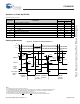
Figure 27. AutoStore or Power-Up RECALL
[23]
V
SWITCH
V
HDIS
t
VCCRISE
t
STORE
t
STORE
t
HHHD
t
HHHD
t
DELAY
t
DELAY
t
LZHSB
t
LZHSB
t
FA
t
FA
HSB OUT
AutoStore
POWER-
UP
RECALL
Read & Write
Inhibited
(RWI)
POWER-UP
RECALL
Read & Write
BROWN
OUT
AutoStore
POWER-UP
RECALL
Read & Write
POWER
DOWN
AutoStore
Note
Note
Note
Note
V
CC
20
20
24
24
Notes
19. t
FA
starts from the time V
CC
rises above V
SWITCH.
20. If an SRAM write has not taken place since the last nonvolatile cycle, no AutoStore or Hardware STORE takes place.
21. On a Hardware STORE and AutoStore initiation, SRAM write operation continues to be enabled for time t
DELAY
.
22. These parameters are guaranteed by design and are not tested.
23. Read and Write cycles are ignored during STORE, RECALL, and while V
CC
is below V
SWITCH.
24. During power-up and power-down, HSB glitches when HSB pin is pulled up through an external resistor.
Not Recommended for New Designs