
Specifications


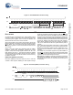


CY14B101P
Document Number: 001-44109 Rev. *O Page 13 of 36
RTC Access
CY14B101P uses 16 registers for RTC. These registers can be
read out or written to by accessing all 16 registers in burst mode
or accessing each register, one at a time. The RDRTC and
WRTC instructions are used to access the RTC.
All the RTC registers can be read in burst mode by issuing the
RDRTC instruction and reading all 16 bytes without bringing the
CS
pin HIGH. The ‘R’ bit must be set while reading the RTC
timekeeping registers to ensure that transitional values of time
are not read.
Writes to the RTC register are performed using the WRTC
instruction. Writing RTC timekeeping registers and control
registers, except for the flags register needs the ‘W’ bit of the
flags register to be set to ‘1’. The internal counters are updated
with the new date and time setting when the ‘W’ bit is cleared to
‘0’. All the RTC registers can also be written in burst mode using
the WRTC instruction.
READ RTC (RDRTC) Instruction
Read RTC (RDRTC) instruction allows the user to read the
contents of RTC registers. Reading the RTC registers through
the SO pin requires the following sequence: After the CS
line is
pulled LOW to select a device, the RDRTC opcode is transmitted
through the SI line followed by eight address bits for selecting the
register. Any data on the SI line after the address bits is ignored.
The data (D7-D0) at the specified address is then shifted out onto
the SO line. RDRTC also allows burst mode read operation.
When reading multiple bytes from RTC registers, the address
rolls over to 0x00 after the last RTC register address (0x0F) is
reached.
The ‘R’ bit in RTC flags register must be set to '1' before reading
RTC time keeping registers to avoid reading transitional data.
Modifying the RTC flags registers requires a Write RTC cycle.
The ‘R’ bit must be cleared to '0' after completion of the read
operation.
The easiest way to read RTC registers is to perform RDRTC in
burst mode. The read may start from the first RTC register (0x00)
and the CS
must be held LOW to allow the data from all 16 RTC
registers to be transmitted through the SO pin.
Note Read RTC (RDRTC) instruction operates at a maximum
clock frequency of 25 MHz. The opcode cycles, address cycles
and data out cycles need to run at 25 MHz for the instruction to
work properly.
Figure 13. Burst Mode Write Instruction Timing
~
~
CS
SCK
SO
MSB
LSB
SI
Op-Code
17-bit Address
MSB
LSB
~
~
~
~
01 234567
0
76 5 432
1
20 21
22 23
01 234567 01 234567
~
~
0
7
0 00000
100000000
A16
A3 A2 A1 A0
HI-Z
Data Byte 1
Data Byte N
D0
D1
D2D3
D4D5D6D7
D0
D1
D2D3
D4D5D6D7
D0D7
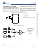
Figure 14. Read RTC (RDRTC) Instruction Timing
CS
SCK
SO
012345 67
0
3
2
1
45 6701234567
MSB LSB
Data
SI
Op-Code
000 1
001
0000
1
A3
A1A2
A0
MSB
LSB
D0
D1
D2D3
D4
D5
D6D7
Not Recommended for New Designs