
User guide


54 Document No. 001-64846 Rev. *A Getting Started with CapSense®
Providing a large shield plane on the PCB sometimes invites radiated emission issues. Ways to reduce emissions
include:
Reduce the size of the shield patterns: The shield electrode pattern should surround the sensor pad and
exposed traces, and spread no further than 1 cm from these features. Spreading the shield electrode beyond 1
cm has negligible effect on system performance. If board space is limited, the shield can spread less than 1cm.
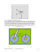
In Figure 3-36 on page 53, Sensor-1 shows an example of a shield pattern surrounding a sensor pad and trace
routed on the top layer. Sensor-2 shows an example of a shield pattern with a sensor pad without a trace on the
top layer.
Drive the shield only when required: In CapSense controllers, when the shield is enabled, it is driven all the
time with a waveform that mirrors the waveform on the sensor pad. Driving the shield only during a scan will
minimize emissions. To drive the shield only during a scan, you need to insert additional code into the firmware.
Limit placement of the shield to select board features: If the shield electrode is being used to reduce
parasitic capacitance, then place the shield only on those sensors that can benefit from reduced C
P
Slow the edges of the shield waveform: The slew rate of shield electrode can be reduced by adding a filter
capacitor between the shield electrode port pin and ground.
. Placing the
shield everywhere will increase emissions without any gain in performance. When scanning a sensor that does
not need the shield electrode, the shield electrode can be disabled in the firmware.