
User guide


50 Document No. 001-64846 Rev. *A Getting Started with CapSense®
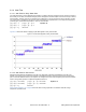
3.7.6 Sensor and Device Placement
Minimize trace length from CapSense controller pins to the sensor pad in order to optimize signal strength.
Series resistors should be mounted within 10 mm of the controller pins to reduce RF interference and provide ESD
protection.
Mount the controller and all other components on the bottom layer of the PCB.
Isolate switching signals such as PWM, I
2
Connectors between the sensor and the controller pins are not recommended since connectors increase C
C communication lines, and LEDs from the sensor and the sensor PCB
traces. Do this by placing them at least 4 mm apart and fill a hatched ground between CapSense traces and non-
CapSense traces to avoid crosstalk.
P
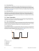
3.7.7 Trace Length and Width
and
decrease noise immunity.
The parasitic capacitance of the traces and sensor pad should be minimized. Trace capacitance is minimized when
they are short and narrow.
Trace length must be less than 12 inches (300 mm) for a standard PCB and less than 2 inches (50 mm) on flex
circuits.
Trace width should be no greater than 7 mil (0.18 mm). CapSense traces should be surrounded by hatched
ground with trace-to-ground clearance of 10 mil to 20 mil (0.25 mm to 0.51 mm).
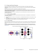
3.7.8 Trace Routing
Route sensor traces on the bottom layer of the PCB. This way the only user interaction with the CapSense sensors is
with the active sensing area. Do not route traces directly under any sensor pad unless the trace is connected to that
sensor.
Do not run capacitive sensing traces in close proximity to communication lines, such as I
2
Figure 3-29
C or SPI masters. If it is
necessary to cross communication lines with sensor pins, make sure the intersection is at right angles, as illustrated
in .
Figure 3-29. Routing of Sensing and Communication Lines