
Specifications


Table Of Contents
- Features
- Description
- Logic Block Diagram
- Contents
- Pin Configurations
- Pin Descriptions
- Absolute Maximum Ratings
- DC Characteristics (VCC = 2.7V-3.6V)
- AC Test Conditions
- Capacitance
- RTC DC Characteristics
- SRAM READ Cycles #1 and #2
- SRAM WRITE Cycles #1 and #2
- AutoStore/Power Up RECALL
- Software-Controlled STORE/RECALL Cycle
- Hardware STORE Cycle
- Soft Sequence Commands
- Mode Selection
- nvSRAM Operation
- Real Time Clock
- RTC Register Map
- Commercial and Industrial Ordering Information
- Ordering Codes
- Package Diagram
- Document History Page
- Sales, Solutions, and Legal Information
STK17T88
Document Number: 001-52040 Rev. *C Page 5 of 24
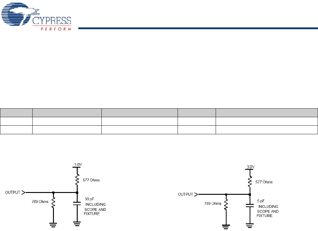
AC Test Conditions
Input Pulse Levels ....................................................0V to 3V
Input Rise and Fall Times .................................................. ≤5 ns
Input and Output Timing Reference Levels ....................1.5V
Output Load..................................See Figure 2 and Figure 3
Capacitance
Figure 2. AC Output Loading Figure 3. AC Output Loading for Tristate Specifications
(T
HZ
, t
LZ
, t
WLQZ
, t
WHQZ
, t
GLQX
, t
GHQZ
)
Symbol Parameter
[2]
Max Units Conditions
C
IN
Input Capacitance 7 pF ΔV = 0 to 3V
C
OUT
Output Capacitance 7 pF ΔV = 0 to 3V
Note
2. These parameters are guaranteed but not tested.
Not Recommended for New Designs
[+] Feedback