
Specifications


Table Of Contents
- Features
- Description
- Logic Block Diagram
- Contents
- Pin Configurations
- Pin Descriptions
- Absolute Maximum Ratings
- DC Characteristics (VCC = 2.7V-3.6V)
- AC Test Conditions
- Capacitance
- RTC DC Characteristics
- SRAM READ Cycles #1 and #2
- SRAM WRITE Cycles #1 and #2
- AutoStore/Power Up RECALL
- Software-Controlled STORE/RECALL Cycle
- Hardware STORE Cycle
- Soft Sequence Commands
- Mode Selection
- nvSRAM Operation
- Real Time Clock
- RTC Register Map
- Commercial and Industrial Ordering Information
- Ordering Codes
- Package Diagram
- Document History Page
- Sales, Solutions, and Legal Information
STK17T88
Document Number: 001-52040 Rev. *C Page 12 of 24
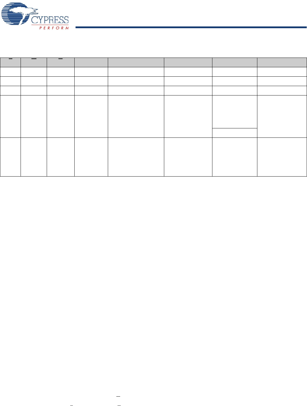
Mode Selection
E W G A
14
-A
0
Mode I/O Power Notes
H X X X Not Selected Output High Z Standby
L H L X Read SRAM Output Data Active
L L X X Write SRAM Input Data Active
LH L0x0E38
0x31C7
0x03E0
0x3C1F
0x303F
Read SRAM
Read SRAM
Read SRAM
Read SRAM
Read SRAM
Output Data
Output Data
Output Data
Output Data
Output Data
Active 17,18,19
0x0FC0 Nonvolatile Store Output High Z I
CC2
LH L0x0E38
0x31C7
0x03E0
0x3C1F
0x303F
0x0C63
Read SRAM
Read SRAM
Read SRAM
Read SRAM
Read SRAM
Nonvolatile Recall
Output Data
Output Data
Output Data
Output Data
Output Data
Output High Z
Active
17,18,19
Notes
17. The six consecutive addresses must be in the order listed. W
must be high during all six consecutive cycles to enable a nonvolatile cycle.
18. While there are 15 addresses on the STK17T88, only the lower 13 are used to control software modes.
19. I/O state depends on the state of G
. The I/O table assumes G low.
Not Recommended for New Designs
[+] Feedback