
nvSRAM Specification Sheet
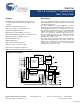
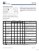
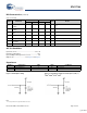
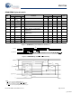
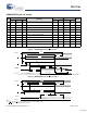
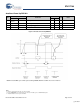
Table Of Contents
- Features
- Description
- Logic Block Diagram
- Pin Configurations
- Pin Descriptions
- Absolute Maximum Ratings
- DC Characteristics
- (VCC = 2.7V-3.6V)
- AC Test Conditions
- Capacitance
- RTC DC Characteristics
- SRAM READ Cycles #1 and #2
- SRAM WRITE Cycles #1 and #2
- AutoStore/Power Up RECALL
- Software-Controlled STORE/RECALL Cycle
- Hardware STORE Cycle
- Soft Sequence Commands
- MODE Selection
- nvSRAM Operation
- Real Time Clock
- RTC Register Map
- Commercial and Industrial Ordering Information
- Ordering Codes
- Package Diagram
- Document History Page
- Sales, Solutions, and Legal Information
STK17T88
Document Number: 001-52040 Rev. *A Page 7 of 22
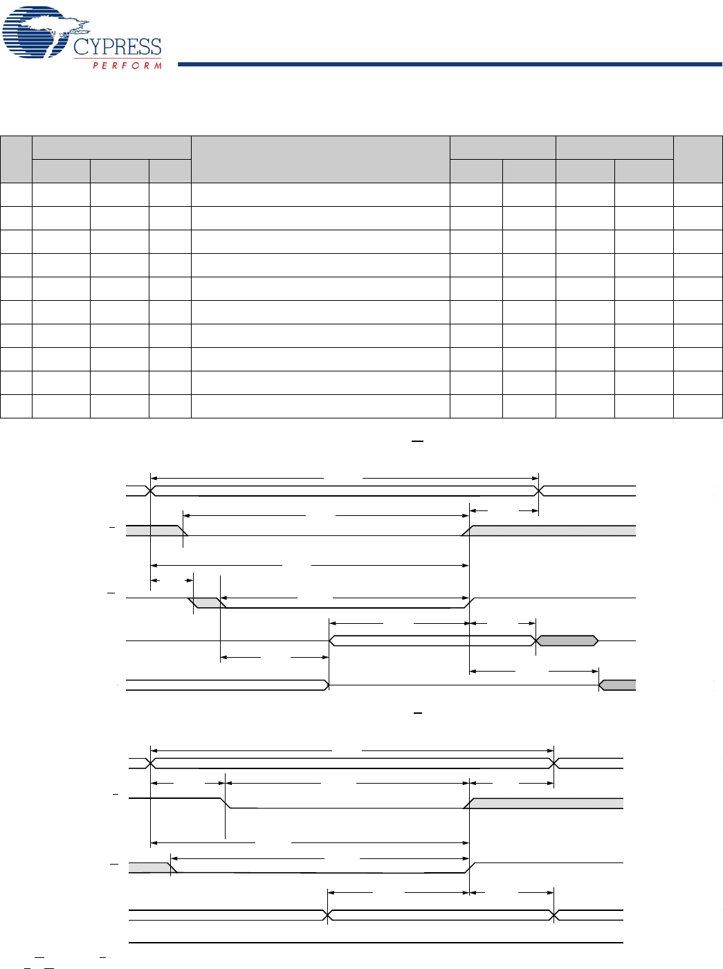
SRAM WRITE Cycles #1 and #2
Figure 7. SRAM WRITE Cycle #1: W Controlled
[7, 8]
Figure 8. SRAM WRITE Cycle #2: E Controlled
[7, 8]
Notes
7. If W
is low when E goes low, the outputs remain in the high-impedance state.
8. E
or W must be ≥ V
IH
durin
g
address transitions.
NO.
Symbols
Parameter
STK17T88-25 STK17T88-45
Units
#1 #2 Alt. Min Max Min Max
12 t
AVAV
t
AVAV
t
WC
Write Cycle Time 25 45 ns
13 t
WLWH
t
WLEH
t
WP
Write Pulse Width 20 30 ns
14 t
ELWH
t
ELEH
t
CW
Chip Enable to End of Write 20 30 ns
15 t
DVWH
t
DVEH
t
DW
Data Set-up to End of Write 10 15 ns
16 t
WHDX
t
EHDX
t
DH
Data Hold after End of Write 0 0 ns
17 t
AVWH
t
AVEH
t
AW
Address Set-up to End of Write 20 30 ns
18 t
AVWL
t
AVEL
t
AS
Address Set-up to Start of Write 0 0 ns
19 t
WHAX
t
EHAX
t
WR
Address Hold after End of Write 0 0 ns
20 t
WLQZ
t
WZ
Write Enable to Output Disable 10 15 ns
21 t
WHQX
t
OW
Output Active after End of Write 3 3 ns
PREVIOUS DATA
DATA OUT
E
ADDRESS
12
t
AVAV
W
16
t
WHDX
DATA IN
19
t
WHAX
13
t
WLWH
18
t
AVWL
17
t
AVWH
DATA VALID
20
t
WLQZ
15
t
DVWH
HIGH IMPEDANCE
21
t
WHQX
14
t
ELWH
DATA IN
12
t
AVAV
16
t
EHDX
13
t
WLEH
19
t
EHAX
18
t
AVEL
17
t
AVEH
DATA VALID
15
t
DVEH
HIGH IMPEDANCE
14
t
ELEH
DATA OUT
E
ADDRESS
W
DATA IN
[+] Feedback