
nvSRAM Specification Sheet
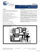
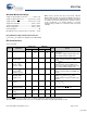
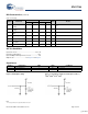
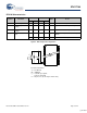
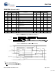
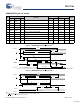
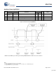
Table Of Contents
- Features
- Description
- Logic Block Diagram
- Pin Configurations
- Pin Descriptions
- Absolute Maximum Ratings
- DC Characteristics
- (VCC = 2.7V-3.6V)
- AC Test Conditions
- Capacitance
- RTC DC Characteristics
- SRAM READ Cycles #1 and #2
- SRAM WRITE Cycles #1 and #2
- AutoStore/Power Up RECALL
- Software-Controlled STORE/RECALL Cycle
- Hardware STORE Cycle
- Soft Sequence Commands
- MODE Selection
- nvSRAM Operation
- Real Time Clock
- RTC Register Map
- Commercial and Industrial Ordering Information
- Ordering Codes
- Package Diagram
- Document History Page
- Sales, Solutions, and Legal Information
STK17T88
Document Number: 001-52040 Rev. *A Page 5 of 22
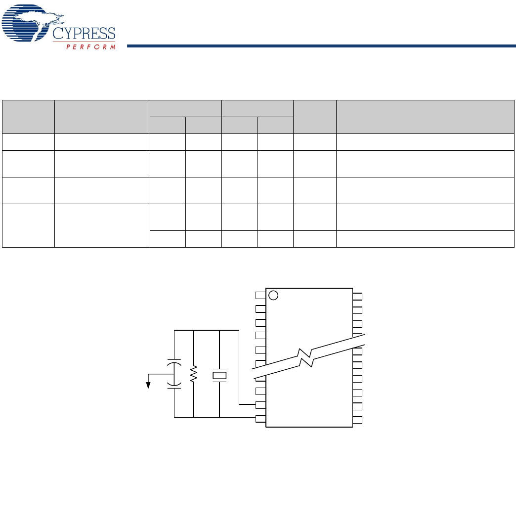
RTC DC Characteristics
Figure 4. RTC Component Configuration
Symbol Parameter
Commercial Industrial
Units Notes
Min Max Min Max
IBAK RTC Backup Current — 300 — 350 nA From either VRTCcap or VRTCbat
VRTCbat RTC Battery Pin
Voltage
1.8 3.3 1.8 3.3 V Typical = 3.0 Volts during normal operation
VRTCcap RTC Capacitor Pin
Voltage
1.2 2.7 1.2 2.7 V Typical = 2.4 Volts during normal operation
tOSCS RTC Oscillator time to
start
— 10 — 10 sec At Minimum Temperature from Power up or
Enable
—5—5secAt 25°C from Power up or Enable
C
1
C
2
RF
Y
1
X
1
X
2
Recommended Values
Y
1
= 32.768 KHz
= 10M Ohm
= 0 (install cap footprint,
but leave unloaded)
= 56 pF ± 10% (do not vary from this value)
RF
C
1
C
2
[+] Feedback