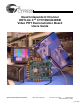
Quad Independent Channel HOTLink II™ CYV15G0404DXB Video PHY Demonstration Board Users Guide Cypress Semiconductor Corporation • 3901 North First Street • San Jose, CA 95134 • 408-943-2600 Revised February 2, 2005 [+] Feedback
Quad Independent Channel HOTLink II™ CYV15G0404DXB Video PHY Demonstration Board TABLE OF CONTENTS 1.0 INTRODUCTION .............................................................................................................................. 5 2.0 KIT CONTENTS ............................................................................................................................... 5 3.0 DEMO BOARD FEATURES ...............................................................................................
Quad Independent Channel HOTLink II™ CYV15G0404DXB Video PHY Demonstration Board LIST OF FIGURES Figure 2-1. Top View of Video Demo Board ............................................................................................ 6 Figure 4-1. Placement of Cable Drivers and Equalizers and Channel-specific LEDs ............................. 7 Figure 4-2. Placement of Clocks on the Board ........................................................................................ 9 Figure 4-3.
Quad Independent Channel HOTLink II™ CYV15G0404DXB Video PHY Demonstration Board LIST OF TABLES Table 4-1. Interface of Cable Drivers and Equalizers to HOTLink II Serial I/Os ..................................... 8 Table 5-1. Summary of GUI Button Functionality (Shown Here for Channel A) ...................................
Quad Independent Channel HOTLink II™ CYV15G0404DXB Video PHY Demonstration Board 1.0 Introduction The Quad Independent Channel HOTLink II CYV15G0404DXB Video Demonstration (Demo) Board is a full-fledged serial digital video reference platform that demonstrates the HOTLink II video physical layers (PHYs) interfacing to industry-standard cable drivers and equalizers. Upstream processing of the video data is performed using on-board Altera Cyclone FPGAs.
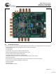
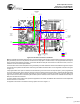
Quad Independent Channel HOTLink II™ CYV15G0404DXB Video PHY Demonstration Board Figure 2-1. Top View of Video Demo Board 3.0 Demo Board Features This section highlights the key features of the Quad Independent Channel HOTLink II CYV15G0404DXB Video PHY Demo Board.
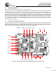
Quad Independent Channel HOTLink II™ CYV15G0404DXB Video PHY Demonstration Board 4.0 Board Architecture The architecture of the board is shown in Figure 4-1 through Figure 4-4. The heart of the board is the Quad Independent Channel HOTLink II CYV15G0404DXB device. The device has four independent transceiver channels. Each transceiver has a transmitter with two outputs and a receiver with two selectable inputs. Each CYV15G0404DXB channel also incorporates a reclocking deserializer.
Quad Independent Channel HOTLink II™ CYV15G0404DXB Video PHY Demonstration Board Table 4-1. Interface of Cable Drivers and Equalizers to HOTLink II Serial I/Os HOTLink II Channel Serial I/O of HOTLink II Device Interfacing Cable Driver Interfacing Equalizer Supported Standard Channel A OUTA1+ Gennum GS1528 x HD-SDI and SD-SDI Channel B Channel C Channel D 4.
Quad Independent Channel HOTLink II™ CYV15G0404DXB Video PHY Demonstration Board Programmable Clocks for Each Channel B C (U13) (U12) D A (U11) (U10) A (X5) B (X2) B (JP13) A (JP11) 74.25 MHz Crystal Oscillators Clock Config Headers for Each D (JP10) Channel C (X4) C (JP12) D (X3) Channel A 27 MHz Crystal 1 to 4 Differential Oscillator (reference for Fanout Clock programmable clocks) (X1) Buffer (U9) Channel B Channel C Channel D Figure 4-2. Placement of Clocks on the Board Note.
Quad Independent Channel HOTLink II™ CYV15G0404DXB Video PHY Demonstration Board JP10, JP11, JP12, JP13 GND 1 5 2 6 3 7 OSC+ 9 GND 13 REFCLKx+ FCLKx+ FCLKx- 10 14 CLOCKOUT+ 11 15 CLOCKOUT- REFCLKx4 8 12 16 GND GND OSC- GND Micrel Programmable Clock SY87729 GND The position of the Micrel programmable clock chip is given to set the correct orientation for determining the pin numbers for clock configuration.
Quad Independent Channel HOTLink II™ CYV15G0404DXB Video PHY Demonstration Board 1. Video test pattern generation. For SD-SDI, the FPGA can generate EG1 Color Bar Data, Grey Pattern, SMPTE RP178, and SMPTE RP178 alternate SDI checkfield patterns. For HD-SDI, the FPGA can generate Color Bar Data, Grey Pattern, SMPTE RP198, and SMPTE RP198 alternate SDI checkfield patterns. 2. Auto rate detection and clock reconfiguration.
Quad Independent Channel HOTLink II™ CYV15G0404DXB Video PHY Demonstration Board Parallel Jumper Headers (JP14, JP15, JP16, JP17, JP18, JP19, JP20, JP21) HOTLink II CYV15G0404DXB (U1) A C B D D C 3-Terminal Positive Regulator (Q2) DC-DC Converter 25W 8V in, 3.3V out (U15) Channel A Channel B Channel C Channel D 6V DC 3-Terminal Positive Regulator (Q1) Power Supply Jack (J1) Figure 4-5. Placement of Power Supply and Jumper Headers 5.
Quad Independent Channel HOTLink II™ CYV15G0404DXB Video PHY Demonstration Board Figure 5-1. Graphical User Interface Table 5-1. Summary of GUI Button Functionality (Shown Here for Channel A) Group Button Name Standard SMPTE Functionality (On Click) No action. This radio button is always selected. 1080i (see channel C in Standard for HD-SDI, automatically checked when user selects 1485Mb/s in Tx/Rx Rate the above figure) Panel of the GUI. NTSC Standard for SD-SDI.
Quad Independent Channel HOTLink II™ CYV15G0404DXB Video PHY Demonstration Board Table 5-1.
Quad Independent Channel HOTLink II™ CYV15G0404DXB Video PHY Demonstration Board If the output is to be viewed on a Tektronix WFM 700 waveform monitor, the user should not select the 360 Mb/s or 540 Mb/s options because this waveform monitor does not support these data rates, and consequently, no images will be displayed on the monitor. Figure 5-2.
Quad Independent Channel HOTLink II™ CYV15G0404DXB Video PHY Demonstration Board Figure 5-5. GUI–Selecting the Standards–HD 5.4 Transmit Test Pattern For SD-SDI, the FPGA can be configured to generate EG1 Color Bar, SMPTE RP178 SDI checkfield, SMPTE RP178 Alternate SDI checkfield, or Grey field patterns. For HD-SDI, the FPGA can be configured to generate Color Bar, SMPTE RP198 SDI checkfield, SMPTE RP198 Alternate SDI checkfield, or Grey field patterns.
Quad Independent Channel HOTLink II™ CYV15G0404DXB Video PHY Demonstration Board Figure 5-7. GUI–Selecting Status 6.0 Sample Test Procedures Before performing the sample tests, please be sure to read Appendix E. It contains instructions on installing the GUI and configuring the hardware completely. Note: The on-board FPGAs and PSoC will be preprogrammed at the factory for testing. Therefore there should be no need to program them. Appendix E contains programming instructions should you need them. 6.
Quad Independent Channel HOTLink II™ CYV15G0404DXB Video PHY Demonstration Board STATUS - Displays video format information and CRC status. Used to see if data contains errors Touchscreen allows easy user interface PICTURE - Displays video EYE - Displays eye diagram used for jitter analysis INPUT - A or B used to choose desired input Figure 6-1. Tektronix WFM 700–Front View S e r ia l D ig ita l In te r fa c e C a r d Channel B in p u t C h a n n e l A in p u t Figure 6-2.
Quad Independent Channel HOTLink II™ CYV15G0404DXB Video PHY Demonstration Board 6.3 Tests This section contains step-by-step tests for fully evaluating the functionality of the board. 6.3.1 Generating SD Color Bar Patterns 1. Apply power to the board and connect the USB cable between the board and the computer. 2. Connect output OUTA1 to input A of the WFM700 using a BNC cable. 3. Open the GUI. 4. Configure channel A to generate color bars in SD format.
Quad Independent Channel HOTLink II™ CYV15G0404DXB Video PHY Demonstration Board Figure 6-4. GUI Setting for Sample Test 1 6.3.2 Generating HD Color Bar Patterns and Reclocking the Data Three Times 1. Apply power to the board and connect the USB cable between the board and the computer. 2. Connect a BNC cable between OUTC1 and IND1, a cable between OUTD1 and INB1, a cable between OUTB1 and INA1, and a cable from OUTA1 to WFM 700.
Quad Independent Channel HOTLink II™ CYV15G0404DXB Video PHY Demonstration Board Figure 6-5.
Quad Independent Channel HOTLink II™ CYV15G0404DXB Video PHY Demonstration Board Figure 6-6. GUI Setting for Sample Test 2 6.3.3 Using Redundant Outputs This test shows that primary input/output of a channel on the board supports both SD-SDI and HD-SDI standards while the secondary input/output supports only the SD-SDI standard (due to presence of SD-SDI equalizers and cable drivers on secondary I/Os). 1. Apply power to the board and connect the USB cable between the board and the computer. 2.
Quad Independent Channel HOTLink II™ CYV15G0404DXB Video PHY Demonstration Board Figure 6-7.
Quad Independent Channel HOTLink II™ CYV15G0404DXB Video PHY Demonstration Board Figure 6-8.
Quad Independent Channel HOTLink II™ CYV15G0404DXB Video PHY Demonstration Board Figure 6-9. GUI Setting for Sample Test 3–Transmit HD-SDI Color Bars 6.3.4 Using Selectable Inputs and Automatic Rate Detection 1. Apply power to the board and connect the USB cable between the board and the computer. 2. Connect OUTB1 to IND2, OUTA1 to IND1, and OUTD1 to input A of the WFM 700. 3. Configure the clock header for channel A to the 74.
Quad Independent Channel HOTLink II™ CYV15G0404DXB Video PHY Demonstration Board 15.View the picture display of the signal on the WFM 700. The user should see the EG1 color bars in SD-SDI format displayed. 16.Press the “Stop” button for all channels. Note: For this test, the clock headers for channel A can be configured to either the on-board programmable clock option or the on-board 74.25-MHz crystal oscillator clock option.
Quad Independent Channel HOTLink II™ CYV15G0404DXB Video PHY Demonstration Board Figure 6-11.
Quad Independent Channel HOTLink II™ CYV15G0404DXB Video PHY Demonstration Board Figure 6-12.
Quad Independent Channel HOTLink II™ CYV15G0404DXB Video PHY Demonstration Board Figure 6-13. GUI Setting for Sample Test 4: Step 13 7.0 Summary The Cypress HOTLink II family of transceivers are compliant to requirements specified by SMPTE for SD-SDI and HD-SDI serial interfaces. The evaluation platform provides a full-fledged reference design that enables customers to easily implement Serial Digital Interface systems with HOTLink II Video PHYs. 8.0 References 1.
Quad Independent Channel HOTLink II™ CYV15G0404DXB Video PHY Demonstration Board Appendix A: Schematics of HOTLink II CYV15G0404DXB Video Demo Board Page 30 of 92 [+] Feedback
D C 1 OUTB1+ OUTB1OUTB2+ OUTB2INB1+ INB1INB2+ INB2OUTC1+ OUTC1OUTC2+ OUTC2INC1+ INC1INC2+ INC2OUTD1+ OUTD1OUTD2+ OUTD2IND1+ IND1IND2+ IND2- OUTB1+ OUTB1OUTB2+ OUTB2INB1+ INB1INB2+ INB2OUTC1+ OUTC1OUTC2+ OUTC2INC1+ INC1INC2+ INC2OUTD1+ OUTD1OUTD2+ OUTD2IND1+ IND1IND2+ IND2- SD/HDA SD/HDB SD/HDC SD/HDD CD/MUTEA CD/MUTEB CD/MUTEC CD/MUTED CD/MUTEB2 CD/MUTED2 SSI/CDC2 OUTA1+ OUTA1OUTA2+ OUTA2INA1+ INA1INA2+ INA2- Flexible Clock &Configuration Flexible Clock &Configuration.
D C B A C36 0.1u C37 0.1u C38 0.1u C39 0.1u 22p C42 22p C41 C40 0.1u Y1 24 MHz 1 1 2 3 4 24LC00 A0 A1 A2 Vss U8 8 7 6 5 I2SCL I2SDA Vcc WP SCL SDA +3.3V R18 2.2K +3.3V R17 2.2K +3.3V C252 0.1u 2 IFCLK DPLUS DMINUS RDY[1..0] C168 0.1u RDY[1..0] C169 0.1u DPLUS/DMINUS should have 90 ohm +/-10% differential impedance. C35 0.1u 2 RDY1 RDY0 C255 0.1u FD[15..0] C254 0.1u R195 1k FD[15..0] C253 0.
D C B A TDO TCLK TDI TMS TMRESET# TD4 1 0 R192 1 TD3 TD1 R15 1.0K R13 1.0K +3.3V R14 1.0K 2 4 6 8 10 HEADER 5X2 1 3 5 7 9 JP9 2 2 +3.3V SCSE1 TXCLKOC TXCLKOD RXDC[7..0] RXDD[7..0] RXSTC[2..0] RXSTD[2..0] RXCLKC+ RXCLKD+ RXCLKCRXCLKDCD/MUTEC CD/MUTED PTXDC[9..0] PTXDD[9..0] F2ASDI F2DCLK F2nCS LFIC LFID CD/MUTED2 SSI/CDC2 F2nCE F2nCONFIG F2CONFIG_DONE PTXCLKC PTXCLKD TXERRC TXERRD TXCLKOA TXCLKOB RXDA[7..0] RXDB[7..0] RXSTA[2..0] RXSTB[2..
D C B A C147 1n 0 FD[15..0] RESET# RXCLKA+ TXCLKOA RXCLKASDI SDO SCSE LFIA INSELB LPENB SCL FD[15..0] CTL[2..0] 1 CLKOUT PA7/*FLAGD/SLCS# TXDA[7..0] TXCTA[1..0] R213 FCLKA+ FCLKA- CTL[2..0] C146 0.1u +1.5VA TXCLKA TXDA[7..0] TXCTA[1..0] C3 C2 D3 D2 D4 D1 E3 E2 F1 E4 E5 F2 F3 F4 F5 G1 G2 F6 F7 G3 G4 G5 G6 H1 H2 H3 H4 H5 H6 J1 H7 J2 J5 J3 J4 K1 J6 K2 J7 K3 K7 L1 K6 K4 K5 L7 L6 L2 L3 L5 L4 M1 M3 M2 M5 M4 N1 N2 M6 N7 N5 N6 N3 N4 P5 P2 P3 R1 P4 R2 R3 T2 T3 + +3.
D C B A RXDD[7..0] RXSTD[2..0] SCL SDO SDI SCSE1 RXCLKD+ TXCLKOD 1 RXDD[7..0] TXERRD RXSTD[2..0] 1n FCLKD+ FCLKD- C151 0.1u RXCLKD- PA7/*FLAGD/SLCS# RESET# CTL[2..0] C150 +1.5VA CTL[2..0] FD[15..0] FD[15..0] C3 C2 D3 D2 D4 D1 E3 E2 F1 E4 E5 F2 F3 F4 F5 G1 G2 F6 F7 G3 G4 G5 G6 H1 H2 H3 H4 H5 H6 J1 H7 J2 J5 J3 J4 K1 J6 K2 J7 K3 K7 L1 K6 K4 K5 L7 L6 L2 L3 L5 L4 M1 M3 M2 M5 M4 N1 N2 M6 N7 N5 N6 N3 N4 P5 P2 P3 R1 P4 R2 R3 T2 T3 + C251 10u C157 0.1u 0.1u 0.1u C185 C156 +3.3V 0.
D C B A 1 1 2 4 6 8 10 12 14 16 18 20 22 2 PTXDC[9..0] PTXDB[9..0] PTXDC[9..0] PTXDB[9..0] PTXDA[9..0] PRXDC[9..0] PRXDB[9..0] PRXDA[9..0] PRXDC[9..0] PRXDB[9..0] PRXDA[9..0] 2 4 6 8 10 12 14 16 18 20 22 HEADER 11X2 1 3 5 7 9 11 13 15 17 19 21 JP20 HEADER 11X2 2 4 6 8 10 12 14 16 18 20 22 PTXCLKD PTXDD0 PTXDD1 PTXDD2 PTXDD3 PTXDD4 PTXDD5 PTXDD6 PTXDD7 PTXDD8 PTXDD9 PTXDD[9..0] PTXDD[9..0] 3 PRXDD[9..0] PRXDD[9..
D C B C279 0.1u +3.3V C281 0.1u +3.3V C278 0.1u +3.3V C280 0.1u +3.3V OUT OUT X1 27 MHz +3.3V 14 VC C GND 7 C283 0.1u C285 0.1u C282 0.1u C284 0.1u 1 8 1 2 1 2 1 2 1 2 C248 0.1u +3.3V 1 NC NC NC NC NC NC NC NC i 50 ohm OUT OUT X3 74.25 MHz OUT OUT X4 74.25 MHz OUT OUT X2 74.25 MHz OUT OUT X5 74.25 MHz i 50 ohm C249 0.1u 6 4 5 4 5 4 5 4 5 R224 130 R228 130 R220 130 R232 130 C140 0.1u +3.3V 1 2 3 4 5 6 7 8 9 10 i i 50 ohm C246 0.
D C B A C167 68u TXCLKOD TXCLKOC TXCLKOB TXCLKOA + 10 R204 10 R203 10 R202 10 R201 1 C227 1u TXCTD[1..0] TXERRD TXCLKD TXDD[7..0] REFCLKD+ REFCLKDSPDSELD TXCTC[1..0] TXERRC TXCLKC TXDC[7..0] REFCLKC+ REFCLKCSPDSELC TXCTB[1..0] TXERRB TXCLKB TXDB[7..0] REFCLKB+ REFCLKBSPDSELB TXCTA[1..0] TXERRA TXCLKA TXDA[7..0] REFCLKA+ REFCLKASPDSELA C228 1u C160 0.1u TXDD[7..0] TXDD7 TXDD6 TXDD5 TXDD4 TXDD3 TXDD2 TXDD1 TXDD0 TXCTD[1..0] TXCTD1 TXCTD0 TXDC[7..
2 3 INA2+ INA2INB2+ INB2INC2+ INC2IND2+ IND2CD/MUTEB2 CD/MUTED2 SSI/CDC2 INA1+ INA1INB1+ INB1INC1+ INC1IND1+ IND1CLIA CLIB CLIC CLID INA2+ INA2INB2+ INB2INC2+ INC2IND2+ IND2CD/MUTEB2 CD/MUTED2 SSI/CDC2 INA1+ INA1INB1+ INB1INC1+ INC1IND1+ IND1CLIA CLIB CLIC CLID 4 5 Linear Systems Ltd. 6 B A B 5 2 6 Revision of 12 G. Cosens LS7652 Sheet 09 Drawn By: Drawing Number Date: 7/6/2004 File: Serial IO Interface.
D C B A OUTD1- OUTD1+ OUTC1- OUTC1+ OUTB1- OUTB1+ OUTA1- OUTA1+ 50 ohm i i 50 ohm 50 ohm i i 50 ohm 50 ohm i i 50 ohm 50 ohm i i 50 ohm R76 100 R71 100 R67 100 R62 100 1 1 R116 750 +3.3V R115 750 +3.3V R114 750 +3.3V R113 750 +3.
D C B A 1 50 ohm i OUTC2+ OUTC2- i 50 ohm 2.2u C92 2.2u Standard C90 50 ohm i OUTD250 ohm i OUTD2+ R157 108.7 R152 40.3 R151 40.3 R156 108.7 R148 52.3 R147 52.3 Optional +5V 0 2.2u R58 0 Optional 2.2u C112 Optional R57 R160 51.1 2 i R60 2.0K R162 51.1 50 ohm +5V 1 2 3 4 50 ohm R163 51.1 R166 1540 R117 750 +5V i 8 7 6 5 8 7 6 5 CLC007 VCC VIN+ VINVEE U29 + +5V Q0 Q0 Q1 Q1 C139 6.8u 1 2 3 4 C89 10n i i 3 75 R94 i 2.2u 75 ohm 2.2u C111 75 ohm 2.
1 C262 68u C263 0.1u C264 0.1u + 2 C265 68u P6 PGood APC08F08 P ENABLE P7 P5 C198 1u 3 + C63 100u 1 2 3 PWR JACK CENTER SLEEVE SHUNT J1 1 IN 3 4 3 +3.3V OUT GND Q1 LM2940CS-5.0 C64 22u IN OUT OUT Q2 LT1587CM-1.5 + +5V 2 4 +1.5V + C66 22u Ferrite Bead L10 + +1.5VA C154 22u LED2 LED2 D28 Linear Systems Ltd. B A B 5 6 Revision of 12 G. Cosens 2 Sheet 12 Drawn By: Drawing Number LS7652 Date: 7/6/2004 File: Power Supply.
Quad Independent Channel HOTLink II™ CYV15G0404DXB Video PHY Demonstration Board Appendix B: PCB Manufacturing Files (GERBER Files) Page 43 of 92 [+] Feedback
Quad Independent Channel HOTLink II™ CYV15G0404DXB Video PHY Demonstration Board Figure B-1.
Quad Independent Channel HOTLink II™ CYV15G0404DXB Video PHY Demonstration Board Figure B-2.
Quad Independent Channel HOTLink II™ CYV15G0404DXB Video PHY Demonstration Board Figure B-3.
Quad Independent Channel HOTLink II™ CYV15G0404DXB Video PHY Demonstration Board Figure B-4.
Quad Independent Channel HOTLink II™ CYV15G0404DXB Video PHY Demonstration Board Figure B-5.
Quad Independent Channel HOTLink II™ CYV15G0404DXB Video PHY Demonstration Board Figure B-6.
Quad Independent Channel HOTLink II™ CYV15G0404DXB Video PHY Demonstration Board Figure B-7.
Quad Independent Channel HOTLink II™ CYV15G0404DXB Video PHY Demonstration Board Figure B-8.
Quad Independent Channel HOTLink II™ CYV15G0404DXB Video PHY Demonstration Board Figure B-9.
Quad Independent Channel HOTLink II™ CYV15G0404DXB Video PHY Demonstration Board Figure B-10.
Quad Independent Channel HOTLink II™ CYV15G0404DXB Video PHY Demonstration Board Figure B-11.
Quad Independent Channel HOTLink II™ CYV15G0404DXB Video PHY Demonstration Board Figure B-12.
Quad Independent Channel HOTLink II™ CYV15G0404DXB Video PHY Demonstration Board Figure B-13.
Quad Independent Channel HOTLink II™ CYV15G0404DXB Video PHY Demonstration Board Figure B-14.
Quad Independent Channel HOTLink II™ CYV15G0404DXB Video PHY Demonstration Board Figure B-15.
Quad Independent Channel HOTLink II™ CYV15G0404DXB Video PHY Demonstration Board Figure B-16.
Quad Independent Channel HOTLink II™ CYV15G0404DXB Video PHY Demonstration Board Figure B-17.
Quad Independent Channel HOTLink II™ CYV15G0404DXB Video PHY Demonstration Board Figure B-18.
Quad Independent Channel HOTLink II™ CYV15G0404DXB Video PHY Demonstration Board Figure B-19.
Quad Independent Channel HOTLink II™ CYV15G0404DXB Video PHY Demonstration Board Figure B-20.
Quad Independent Channel HOTLink II™ CYV15G0404DXB Video PHY Demonstration Board Figure B-21.
Quad Independent Channel HOTLink II™ CYV15G0404DXB Video PHY Demonstration Board Appendix C: PCB Assembly Files (Drill and Assembly) Page 65 of 92 [+] Feedback
Quad Independent Channel HOTLink II™ CYV15G0404DXB Video PHY Demonstration Board Figure C-1.
Quad Independent Channel HOTLink II™ CYV15G0404DXB Video PHY Demonstration Board Figure C-2.
Quad Independent Channel HOTLink II™ CYV15G0404DXB Video PHY Demonstration Board Figure C-3.
Quad Independent Channel HOTLink II™ CYV15G0404DXB Video PHY Demonstration Board Appendix D: Bill of Materials (BOM) of HOTLink II CYV15G0404DXB Video Demo Board Page 69 of 92 [+] Feedback
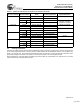
Quad Independent Channel HOTLink II™ CYV15G0404DXB Video PHY Demonstration Board Table D-1. Bill of Materials for HOTLink II CYV15G0404DXB Video Demo Board Qty Part No. Manufacturer Description Designator 185 C0603C104K4RAC Kemet 0.
Quad Independent Channel HOTLink II™ CYV15G0404DXB Video PHY Demonstration Board Table D-1. Bill of Materials for HOTLink II CYV15G0404DXB Video Demo Board (continued) Qty Part No. Manufacturer Description Designator 43 ECJ-1VB0J225K Panasonic CAP 2.2-µF 6.
Quad Independent Channel HOTLink II™ CYV15G0404DXB Video PHY Demonstration Board Table D-1. Bill of Materials for HOTLink II CYV15G0404DXB Video Demo Board (continued) Qty Part No.
Quad Independent Channel HOTLink II™ CYV15G0404DXB Video PHY Demonstration Board Table D-1. Bill of Materials for HOTLink II CYV15G0404DXB Video Demo Board (continued) Qty Part No. Manufacturer Panasonic Description Designator 36 ERJ-3EKF75R0V 1 CYV15G0404DXB-BGC Cypress Independent Clock Quad HOTLink II U1 Transceiver 4 SY87729LHI 3.3V AnyClock Fractional N Synthesizer U10, U11, U12, U13 1 CY8C27643-24PVI Cypress PSoC Mixed Signal Array 1 APC08F08 Astec CONV DC-DC 25W 8VIN 3.
Quad Independent Channel HOTLink II™ CYV15G0404DXB Video PHY Demonstration Board Table D-1. Bill of Materials for HOTLink II CYV15G0404DXB Video Demo Board (continued) Qty Part No.
Quad Independent Channel HOTLink II™ CYV15G0404DXB Video PHY Demonstration Board Appendix E: Unpacking HOTLink II CYV15G0404DXB Video Demo Board Page 75 of 92 [+] Feedback
Quad Independent Channel HOTLink II™ CYV15G0404DXB Video PHY Demonstration Board The software GUI must be installed from the resource CD included in the kit. Please follow instructions listed below for installing and running the various tests from the GUI. HOTLink II CYV15G0404DXB Video Demo Board Software Set-up Instructions Open the CD that was supplied with the kit and locate the file named “HOTLink II Video Demo Board Set-up.exe” located in the zip file.
Quad Independent Channel HOTLink II™ CYV15G0404DXB Video PHY Demonstration Board Figure E-3. Software Set-up Wizard 2 5. Select the Start menu folder in which the HOTLink II Video Demo Board shortcut will be created, then click on “Next.” Figure E-4.
Quad Independent Channel HOTLink II™ CYV15G0404DXB Video PHY Demonstration Board 6. Click on the check box to have the software icon installed either on desktop, or as a quick launch icon, or both, then click “Next.” Figure E-5. Software Set-up Wizard 4 7. Click install to have the software installed. Figure E-6.
Quad Independent Channel HOTLink II™ CYV15G0404DXB Video PHY Demonstration Board The HVDB icon will now be available on your Desktop and/or as a Quick Launch item in your taskbar (depending on your selections during installation). Connect the 6V DC power supply to the power supply jack (J1) on the board. The power LEDs on the board will turn on. Connect the USB cable between the USB port of the video board and the PC/laptop.
Quad Independent Channel HOTLink II™ CYV15G0404DXB Video PHY Demonstration Board 3. “Completing the Find New Hardware Wizard” will pop up. Click on “Finish.” Figure E-9. New Hardware Wizard 2 4. Click on the HVDB icon on your desktop or Quick Launch taskbar. The HVDB GUI should appear as shown in Figure E-15 indicating that and you have successfully installed the relevant software and hardware on the computer.
Quad Independent Channel HOTLink II™ CYV15G0404DXB Video PHY Demonstration Board Figure E-11. Add Hardware Wizard 6. Make sure the USB cable is connected to the PC/laptop at this point. The “Yes, I have already connected the hardware” option should be checked by default. Click on “Next.” Figure E-12.
Quad Independent Channel HOTLink II™ CYV15G0404DXB Video PHY Demonstration Board 7. Select the “Cypress HOTLink II Video Demo Board” hardware already installed on the computer. Figure E-13. Add Hardware Wizard 3 8. Click on “Finish” when the hardware is configured properly. Figure E-14.
Quad Independent Channel HOTLink II™ CYV15G0404DXB Video PHY Demonstration Board • The GUI looks like the following. Figure E-15. HVDB Graphical User Interface Board Configuration Instructions Please note that the FPGAs and PSoC are preprogrammed at the factory, for testing purposes. Therefore, you should have no need to perform the following steps. They are included as a reference should you ever need to reprogram the board. 1. Double click on the HDVB icon. The GUI should appear. 2.
Quad Independent Channel HOTLink II™ CYV15G0404DXB Video PHY Demonstration Board Figure E-17. FPGA Programming Dialog Box 1 Figure E-18. FPGA Programming Dialog Box 2 Figure E-19. FPGA Programming Dialog Box 3 Click on FPGA2 (U3). This will bring up a “File Open” dialog box. Select “Hdvb1.pof.” Click on “Open.” The FPGA is configured the same way as in (1). 3. Click on Tools->PSoC Programming. A small dialog should pop up as shown. Click on “Program PSoC.” This will bring up a File Open dialog box.
Quad Independent Channel HOTLink II™ CYV15G0404DXB Video PHY Demonstration Board Setting Configurations Once the user has configured the desired settings on the GUI, the settings selected can be saved to a file for future retrieval. Similarly, a user can retrieve a saved setting. • To save a current setting, click on File -> Save Settings, the “Save As” dialog box will prompt the user to enter a valid file name and the setting for the GUI is saved as a configuration file with an “.ini” file extension.
Quad Independent Channel HOTLink II™ CYV15G0404DXB Video PHY Demonstration Board Appendix F: Configuring the HOTLink II CYV15G0404DXB Video Demo Board for SD-SDI to HD-SDI Upconversion Page 86 of 92 [+] Feedback
Quad Independent Channel HOTLink II™ CYV15G0404DXB Video PHY Demonstration Board Overview This appendix discusses the necessary modifications that need to be made to the CYV15G0404DXB video demo board, in order for it to be able to perform upconversion. The upconversion function described in this appendix is for functional verification only. Due to design constraints, the measured jitter will be higher than normal. If you have any questions about this feature please contact Cypress’s Application Engineers.
Quad Independent Channel HOTLink II™ CYV15G0404DXB Video PHY Demonstration Board Clock Rate Conversion As part of the upconversion process, the incoming SDI clock rate (27 MHz) must be converted to HD-SDI (half rate at 74.25/1.001 MHz). To achieve this, both PLLs in FPGA(U2) are connected in series to get the correct frequency for transmitting. The 27-MHz clock rate from RXCLKB+ is passed through FPGA(U2), where the first PLL multiplies RXCLKB+ by 25/13, while the second PLL multiplies the result by 10/7.
Quad Independent Channel HOTLink II™ CYV15G0404DXB Video PHY Demonstration Board 2.Remove resistor R205. The RXCLKA+ pin on FPGA(U2) is connected to the input of the second PLL in FPGA(U2). However, the RXCLKA+ output pin of the CYV15G0404DXB chip is connected to the RXCLKA+ input pin of FPGA(U2). The removal of resistor R205 breaks this connection and allows FCLKB to be routed through the second PLL. 3. .Configure clocking options to FPGA clock option for Channel A (JP11).
Quad Independent Channel HOTLink II™ CYV15G0404DXB Video PHY Demonstration Board OUTB2 INB2 OUTB1 INB1 OUTA1 INA1 MS Windows based PC OUTD2 IND2 Tektronix WFM 700 OUTD1 IND1 INC1 OUTC1 INC2 OUTC2 Figure F-5. Upconversion Test Connections GUI Configuration Configuration of the CYV15G0404DXB GUI is comprised of the following steps. The typical settings are shown in Figure F-6. 1. Enable an SD-SDI/SMPTE 259M-C signal by selecting 270 Mb/s in the Tx/Rx Rate Box of the GUI. 2.
Quad Independent Channel HOTLink II™ CYV15G0404DXB Video PHY Demonstration Board Figure F-6.
Quad Independent Channel HOTLink II™ CYV15G0404DXB Video PHY Demonstration Board Results The output of the upconverted signal may be verified by monitoring the output signal on any HD-SDI waveform monitor (example Tektronix WFM 700). Figure F-7 and Figure F-8 show the output for an SD-SDI, HD-HDI, and upconverted HD-SDI signal respectively. Figure F-7. SD-SDI Video Picture Figure F-8. Upconverted HD-SDI Video Picture Unused active video samples in active outgoing video lines are set to black.