
Specifications


CY8C21123/CY8C21223/CY8C21323
Document Number: 38-12022 Rev. *Y Page 9 of 46
Table 4. Pin Definitions – CY8C21223 16-Pin QFN with no E-Pad
[3]
Pin
No.
Type
Pin
Name
Description
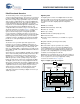
Figure 5. CY8C21223 16-Pin QFN
Digital Analog
1 I/O I P0[3] Analog column mux input
2 I/O I P0[1] Analog column mux input
3 I/O P1[7] I
2
C SCL
4 I/O P1[5] I
2
C SDA
5 I/O P1[3]
6 I/O P1[1] I
2
C SCL, ISSP-SCLK
[3]
7 Power V
SS
Ground connection
8 I/O P1[0] I
2
C SDA, ISSP-SDATA
[3]
9 I/O P1[6]
10 I/O P1[4] EXTCLK
11 Input XRES Active high external reset with internal
pull-down
12 I/O I P0[4] V
REF
13 Power V
DD
Supply voltage
14 I/O I P0[7] Analog column mux input
15 I/O I P0[5] Analog column mux input
16 NC No Connection. Pin must be left floating
LEGEND A = Analog, I = Input, and O = Output.
QFN
(
Top View
)
1
2
3
4
12
11
10
9
5
6
7
8
13
14
15
16
P0[4], V
REF
P0[5], AI
P0[7], AI
V
DD
P1[3]
I2C SCL, P1[1]
V
SS
I2C SDA, P1[0]
XRES
P1[4]
P1[6]
AI, P0[3]
AI, P0[1]
I2C SCL, P1[7]
I2C SDA, P1[5]
NC
Notes
3. These are the ISSP pins, which are not high Z at POR (power on reset). See the PSoC Technical Reference Manual for details.
4. The center pad on the QFN package must be connected to ground (Vss) for best mechanical, thermal, and electrical performance. If not connected to ground, it
must be electrically floated and not connected to any other signal.