
Specifications


CY8C21123/CY8C21223/CY8C21323
Document Number: 38-12022 Rev. *Y Page 4 of 46
Analog System
The analog system consists of four configurable blocks to allow
creation of complex analog signal flows. Analog peripherals are
very flexible and may be customized to support specific
application requirements. Some of the more common PSoC
analog functions (most available as user modules) are:
■ Analog-to-digital converters (single or dual, with 8-bit or 10-bit
resolution)
■ Pin-to-pin comparators (one)
■ Single-ended comparators (up to 2) with absolute (1.3 V)
reference or 8-bit DAC reference
■ 1.3 V reference (as a system resource)
In most PSoC devices, analog blocks are provided in columns of
three, which includes one CT (continuous time) and two SC
(switched capacitor) blocks. The CY8C21x23 devices provide
limited functionality Type “E” analog blocks. Each column
contains one CT block and one SC block.
The number of blocks on the device family is listed in Table 1 on
page 5.
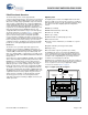
Figure 2. CY8C21x23 Analog System Block Diagram
Additional System Resources
System resources, some of which listed in the previous sections,
provide additional capability useful to complete systems.
Additional resources include a switch mode pump, low voltage
detection, and power on reset. The merits of each system
resource are.
■ Digital clock dividers provide three customizable clock
frequencies for use in applications. The clocks can be routed
to both the digital and analog systems. Additional clocks can
be generated using digital PSoC blocks as clock dividers.
■ The I
2
C module provides 100 and 400 kHz communication over
two wires. Slave, master, and multi-master modes are all
supported.
■ LVD interrupts can signal the application of falling voltage
levels, while the advanced POR (power on reset) circuit
eliminates the need for a system supervisor.
■ An internal 1.3 V voltage reference provides an absolute
reference for the analog system, including ADCs and DACs.
■ An integrated switch mode pump (SMP) generates normal
operating voltages from a single 1.2 V battery cell, providing a
low cost boost converter.
ACOL1M UX
ACE00 ACE01
Array
Array Input
Configuration
ACI0[1:0] ACI1[1:0]
ASE10 ASE11