
Specifications


CY8C21123/CY8C21223/CY8C21323
Document Number: 38-12022 Rev. *Y Page 3 of 46
PSoC Functional Overview
The PSoC family consists of many programmable
system-on-chip controller devices. These devices are designed
to replace multiple traditional MCU-based system components
with a low cost single-chip programmable component. A PSoC
device includes configurable blocks of analog and digital logic,
and programmable interconnect. This architecture allows you to
create customized peripheral configurations, to match the
requirements of each individual application. Additionally, a fast
CPU, Flash program memory, SRAM data memory, and
configurable I/O are included in a range of convenient pinouts.
The PSoC architecture, as shown in Figure 1, consists of four
main areas: the Core, the System Resources, the Digital
System, and the Analog System. Configurable global bus
resources allow the combining of all device resources into a
complete custom system. Each PSoC device includes four digital
blocks. Depending on the PSoC package, up to two analog
comparators and up to 16 GPIO are also included. The GPIO
provide access to the global digital and analog interconnects.
PSoC Core
The PSoC Core is a powerful engine that supports a rich
instruction set. It encompasses SRAM for data storage, an
interrupt controller, sleep and watchdog timers, and internal main
oscillator (IMO), and internal low-speed oscillator (ILO). The
CPU core, called the M8C, is a powerful processor with speeds
up to 24 MHz. The M8C is a four MIPS 8-bit Harvard-architecture
microprocessor.
System Resources provide additional capability, such as digital
clocks or I
2
C functionality for implementing an I
2
C master, slave,
MultiMaster, an internal voltage reference that provides an
absolute value of 1.3 V to a number of PSoC subsystems, an
SMP that generates normal operating voltages off a single
battery cell, and various system resets supported by the M8C.
The digital system consists of an array of digital PSoC blocks,
which can be configured into any number of digital peripherals.
The digital blocks can be connected to the GPIO through a series
of global bus that can route any signal to any pin. This frees
designs from the constraints of a fixed peripheral controller.
The analog system consists of four analog PSoC blocks,
supporting comparators and analog-to-digital conversion up to
10 bits of precision.
Digital System
The digital system consists of four digital PSoC blocks. Each
block is an 8-bit resource that can be used alone or combined
with other blocks to form 8, 16, 24, and 32-bit peripherals, which
are called user modules. Digital peripheral configurations
include:
■ PWMs (8- and 16-bit)
■ PWMs with dead band (8- and 16-bit)
■ Counters (8- to 32-bit)
■ Timers (8- to 32-bit)
■ UART 8-bit with selectable parity (up to two)
■ SPI master and slave
■ I
2
C slave, master, multi-master (one available as a system
resource)
■ Cyclical redundancy checker/generator (8-bit)
■ IrDA (up to two)
■ Pseudo random sequence generators (8- to 32-bit)
The digital blocks can be connected to any GPIO through a
series of global bus that can route any signal to any pin. The
busses also allow for signal multiplexing and performing logic
operations. This configurability frees your designs from the
constraints of a fixed peripheral controller.
Digital blocks are provided in rows of four, where the number of
blocks varies by PSoC device family. This provides an optimum
choice of system resources for your application. Family
resources are shown in Table 1 on page 5.
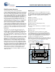
Figure 1. Digital System Block Diagram
DIGITAL SYSTEM
To System Bus
D
i
g
i
t
a
l
C
l
o
c
k
s
F
r
o
m
C
o
r
e
Di gi ta l P S oC Bl o ck Arr a y
To Anal og
System
8
Row Input
Configuration
Row Output
Configuration
88
8
Row 0
DBB00 DBB01 DCB02 DCB03
4
4
GIE[7:0]
GIO[7:0]
GOE[7:0]
GOO[7:0]
Global Digital
Interconnect
Port 1
Port 0