
Specifications


CY8C21123/CY8C21223/CY8C21323
Document Number: 38-12022 Rev. *Y Page 11 of 46
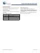
24-Pin Part Pinout
Table 6. Pin Definitions – CY8C21323 24-Pin QFN
[5]
Pin
No.
Type
Pin
Name
Description
Figure 7. CY8C21323 24-Pin QFN
Digital Analog
1 I/O I P0[1] Analog column mux input
2 Power SMP SMP connection to required external
components
3 Power V
SS
Ground connection
4 I/O P1[7] I
2
C SCL
5 I/O P1[5] I
2
C SDA
6 I/O P1[3]
7 I/O P1[1] I
2
C SCL, ISSP-SCLK
[3]
8 NC No connection. Pin must be left floating
9 Power V
SS
Ground connection
10 I/O P1[0] I
2
C SDA, ISSP-SDATA
[3]
11 I/O P1[2]
12 I/O P1[4] Optional (EXTCLK) input
13 I/O P1[6]
14 Input XRES Active high external reset with internal
pull-down
15 NC No connection. Pin must be left floating
16 I/O I P0[0] Analog column mux input
17 I/O I P0[2] Analog column mux input
18 I/O I P0[4] Analog column mux input
19 I/O I P0[6] Analog column mux input
20 Power V
DD
Supply voltage
21 Power V
SS
Ground connection
22 I/O I P0[7] Analog column mux input
23 I/O I P0[5] Analog column mux input
24 I/O I P0[3] Analog column mux input
LEGEND A = Analog, I = Input, and O = Output.
QFN
(Top View)
A, I, P0[1]
SMP
V
SS
I2C SCL, P1[7]
I2C SDA, P1[5]
P1[3]
1
2
3
4
5
6
18
17
16
15
14
13
P0[4], A, I
P0[2], A, I
NC
XRES
P1[6]
24
23
22
21
20
19
P0[3], A, I
P0[5], A, I
P0[7], A, I
V
SS
V
DD
P0[6], A, I
7
8
9
10
11
12
I2C SCL, P1[1]
NC
V
SS
I2C SDA, P1[0]
P1[2]
EXTCLK, P1[4]
P0[0], A, I
Note
5. The center pad on the QFN package must be connected to ground (V
SS
) for best mechanical, thermal, and electrical performance. If not connected to ground, it
must be electrically floated and not connected to any other signal.