
Specifications


CY8C21123/CY8C21223/CY8C21323
Document Number: 38-12022 Rev. *Y Page 10 of 46
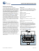
20-Pin Part Pinout
Table 5. Pin Definitions – CY8C21323 20-Pin SSOP
Pin
No.
Type
Pin
Name
Description
Figure 6. CY8C21323 20-Pin SSOP
Digital Analog
1 I/O I P0[7] Analog column mux input
2 I/O I P0[5] Analog column mux input
3 I/O I P0[3] Analog column mux input
4 I/O I P0[1] Analog column mux input
5 Power V
SS
Ground connection
6 I/O P1[7] I
2
C SCL
7 I/O P1[5] I
2
C SDA
8 I/O P1[3]
9 I/O P1[1] I
2
C SCL, ISSP-SCLK
[3]
10 Power V
SS
Ground connection
11 I/O P1[0] I
2
C SDA, ISSP-SDATA
[3]
12 I/O P1[2]
13 I/O P1[4] Optional EXTCLK input
14 I/O P1[6]
15 Input XRES Active high external reset with internal
pull-down
16 I/O I P0[0] Analog column mux input
17 I/O I P0[2] Analog column mux input
18 I/O I P0[4] Analog column mux input
19 I/O I P0[6] Analog column mux input
20 Power V
DD
Supply voltage
LEGEND A = Analog, I = Input, and O = Output.
SSOP
V
DD
P0[6], A, I
P0[4], A, I
P0[2], A, I
P0[0], A, I
XRES
P1[6]
P1[4], EXTCLK
P1[2]
P1[0], I2C SDA
20
19
18
17
16
15
14
13
12
11
1
2
3
4
5
6
7
8
9
10
A, I, P0[7]
A, I, P0[5]
A, I, P0[3]
A, I, P0[1]
I2C SCL, P1[7]
I2C SDA, P1[5]
P1[3]
I2C SCL, P1[1]
V
SS
V
SS