CY8C21123/CY8C21223/CY8C21323 PSoC® Programmable System-on-Chip™ PSoC® Programmable System-on-Chip™ Features ❐ ■ Powerful Harvard-architecture processor: ❐ M8C processor speeds up to 24 MHz ❐ Low power at high speed ❐ Operating voltage: 2.4 V to 5.25 V ❐ Operating voltages down to 1.
CY8C21123/CY8C21223/CY8C21323 Contents PSoC Functional Overview .............................................. 3 PSoC Core .................................................................. 3 Digital System ............................................................. 3 Analog System ............................................................ 4 Additional System Resources ..................................... 4 PSoC Device Characteristics ...................................... 5 Getting Started ..........
CY8C21123/CY8C21223/CY8C21323 PSoC Functional Overview The PSoC family consists of many programmable system-on-chip controller devices. These devices are designed to replace multiple traditional MCU-based system components with a low cost single-chip programmable component. A PSoC device includes configurable blocks of analog and digital logic, and programmable interconnect.
CY8C21123/CY8C21223/CY8C21323 Analog System Additional System Resources The analog system consists of four configurable blocks to allow creation of complex analog signal flows. Analog peripherals are very flexible and may be customized to support specific application requirements. Some of the more common PSoC analog functions (most available as user modules) are: System resources, some of which listed in the previous sections, provide additional capability useful to complete systems.
CY8C21123/CY8C21223/CY8C21323 PSoC Device Characteristics Depending on your PSoC device characteristics, the digital and analog systems can have 16, 8, or 4 digital blocks, and 12, 6, or 4 analog blocks. Table 1 lists the resources available for specific PSoC device groups. The PSoC device covered by this datasheet is highlighted. Table 1.
CY8C21123/CY8C21223/CY8C21323 Development Tool Selection Software PSoC Designer At the core of the PSoC development software suite is PSoC Designer. Utilized by thousands of PSoC developers, this robust software has been facilitating PSoC designs for years. PSoC Designer is available free of charge at http://www.cypress.com. PSoC Designer comes with a free C compiler.
CY8C21123/CY8C21223/CY8C21323 Designing with PSoC Designer The development process for the PSoC device differs from that of a traditional fixed function microprocessor. The configurable analog and digital hardware blocks give the PSoC architecture a unique flexibility that pays dividends in managing specification change during development and by lowering inventory costs. These configurable resources, called PSoC Blocks, have the ability to implement a wide variety of user-selectable functions.
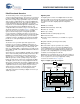
CY8C21123/CY8C21223/CY8C21323 Pin Information This section describes, lists, and illustrates the CY8C21x23 PSoC device pins and pinout configurations. Every port pin (labeled with a “P”) is capable of Digital I/O. However, VSS, VDD, SMP, and XRES are not capable of Digital I/O. 8-Pin Part Pinout Table 2. Pin Definitions – CY8C21123 8-Pin SOIC Pin No.
CY8C21123/CY8C21223/CY8C21323 Table 4.
CY8C21123/CY8C21223/CY8C21323 20-Pin Part Pinout Table 5. Pin Definitions – CY8C21323 20-Pin SSOP Pin No.
CY8C21123/CY8C21223/CY8C21323 24-Pin Part Pinout Table 6. Pin Definitions – CY8C21323 24-Pin QFN[5] 15 16 17 18 19 20 21 22 23 24 Input I/O I/O I/O I/O I I I I Power Power I/O I/O I/O I I I NC P0[0] P0[2] P0[4] P0[6] VDD VSS P0[7] P0[5] P0[3] P0[7], A, I VSS VDD P0[6], A, I 20 19 P0[3], A, I P0[5], A, I 18 17 QFN 16 (Top View) 15 14 13 11 12 Optional (EXTCLK) input 1 2 3 4 5 6 P1[2] EXTCLK, P1[4] Power I/O I/O I/O I/O I2C SCL, ISSP-SCLK[3] No connection.
CY8C21123/CY8C21223/CY8C21323 Register Reference This section lists the registers of the CY8C21x23 PSoC device. For detailed register information, refer the PSoC Technical Reference Manual. Register Conventions The register conventions specific to this section are listed in the following table. Table 7. Register Conventions Convention Register Mapping Tables The PSoC device has a total register address space of 512 bytes. The register space is referred to as I/O space and is divided into two banks.
CY8C21123/CY8C21223/CY8C21323 Table 8.
CY8C21123/CY8C21223/CY8C21323 Table 8.
CY8C21123/CY8C21223/CY8C21323 Table 9.
CY8C21123/CY8C21223/CY8C21323 Electrical Specifications This section presents the DC and AC electrical specifications of the CY8C21x23 PSoC device. For up to date electrical specifications, check if you have the latest datasheet by visiting the web at http://www.cypress.com. Specifications are valid for –40 °C TA 85 °C and TJ 100 °C, except where noted. Refer to Table 24 on page 25 for the electrical specifications on the IMO using SLIMO mode. 5.25 SLIMO Mode = 0 Figure 11.
CY8C21123/CY8C21223/CY8C21323 Operating Temperature Table 11. Operating Temperature Symbol TA TJ Description Ambient temperature Junction temperature Min –40 –40 Typ – – Max +85 +100 Units °C °C Notes The temperature rise from ambient to junction is package specific. SeeTable 36 on page 34. You must limit the power consumption to comply with this requirement.
CY8C21123/CY8C21223/CY8C21323 DC GPIO Specifications Table 13 lists the guaranteed maximum and minimum specifications for the voltage and temperature ranges: 4.75 V to 5.25 V and –40 °C TA 85 °C, 3.0 V to 3.6 V and –40 °C TA 85 °C, respectively. Typical parameters apply to 5 V, 3.3 V, or 2.7 V at 25 °C and are for design guidance only. Table 13. 5-V and 3.3-V DC GPIO Specifications Symbol Description Pull-up resistor RPU Pull-down resistor RPD High output level VOH Min 4 4 VDD – 1.0 Typ 5.6 5.
CY8C21123/CY8C21223/CY8C21323 DC Amplifier Specifications The following tables list the guaranteed maximum and minimum specifications for the voltage and temperature ranges: 4.75 V to 5.25 V and –40 °C TA 85 °C, 3.0 V to 3.6 V and –40 °C TA 85 °C, or 2.4 V to 3.0 V and –40 °C TA 85 °C, respectively. Typical parameters apply to 5 V, 3.3 V, or 2.7 V at 25 °C and are for design guidance only. Table 15.
CY8C21123/CY8C21223/CY8C21323 DC Switch Mode Pump Specifications Table 18 lists the guaranteed maximum and minimum specifications for the voltage and temperature ranges: 4.75 V to 5.25 V and –40 °C TA 85 °C, 3.0 V to 3.6 V and –40 °C TA 85 °C, or 2.4 V to 3.0 V and –40 °C TA 85 °C, respectively. Typical parameters apply to 5 V, 3.3 V, or 2.7 V at 25 °C and are for design guidance only. Table 18.
CY8C21123/CY8C21223/CY8C21323 Figure 12. Basic Switch Mode Pump Circuit D1 Vdd V DD L1 V BAT + V PUMP C1 SMP Battery PSoCTM V ss DC POR and LVD Specifications Table 19 lists the guaranteed maximum and minimum specifications for the voltage and temperature ranges: 4.75 V to 5.25 V and –40 °C TA 85 °C, 3.0 V to 3.6 V and –40 °C TA 85 °C, or 2.4 V to 3.0 V and –40 °C TA 85 °C, respectively. Typical parameters apply to 5 V, 3.3 V, or 2.7 V at 25 °C and are for design guidance only. Table 19.
CY8C21123/CY8C21223/CY8C21323 DC Programming Specifications Table 20 lists the guaranteed maximum and minimum specifications for the voltage and temperature ranges: 4.75 V to 5.25 V and –40 °C TA 85 °C, 3.0 V to 3.6 V and –40 °C TA 85 °C, or 2.4 V to 3.0 V and –40 °C TA 85 °C, respectively. Typical parameters apply to 5 V, 3.3 V, or 2.7 V at 25 °C and are for design guidance only. Table 20. DC Programming Specifications Symbol VDDP Description VDD for programming and erase Min 4.5 Typ 5.
CY8C21123/CY8C21223/CY8C21323 AC Electrical Characteristics AC Chip-Level Specifications Table 22 lists the guaranteed maximum and minimum specifications for the voltage and temperature ranges: 4.75 V to 5.25 V and –40 °C TA 85 °C, 3.0 V to 3.6 V and –40 °C TA 85 °C, or 2.4 V to 3.0 V and –40 °C TA 85 °C, respectively. Typical parameters apply to 5 V, 3.3 V, or 2.7 V at 25 °C and are for design guidance only. Table 22. 5-V and 3.
CY8C21123/CY8C21223/CY8C21323 Table 23. 2.7-V AC Chip-Level Specifications Min Typ Max Units FIMO12 Symbol IMO frequency for 12 MHz Description 11.5 120 12.7[19,20] MHz Trimmed for 2.7 V operation using factory trim values. See Figure 11 on page 16. SLIMO mode = 1. FIMO6 IMO frequency for 6 MHz 5.5 6 6.5[19,20] MHz Trimmed for 2.7 V operation using factory trim values. See Figure 11 on page 16. SLIMO mode = 1. FCPU1 CPU frequency (2.7 V nominal) 0.093 3 3.
CY8C21123/CY8C21223/CY8C21323 AC General Purpose I/O Specifications Table 24 lists the guaranteed maximum and minimum specifications for the voltage and temperature ranges: 4.75 V to 5.25 V and –40 °C TA 85 °C, 3.0 V to 3.6 V and –40 °C TA 85 °C, or 2.4 V to 3.0 V and –40 °C TA 85 °C, respectively. Typical parameters apply to 5 V, 3.3 V, or 2.7 V at 25 °C and are for design guidance only. Table 24. 5-V and 3.
CY8C21123/CY8C21223/CY8C21323 AC Digital Block Specifications Table 28 lists the guaranteed maximum and minimum specifications for the voltage and temperature ranges: 4.75 V to 5.25 V and –40 °C TA 85 °C, 3.0 V to 3.6 V and –40 °C TA 85 °C, or 2.4 V to 3.0 V and –40 °C TA 85 °C, respectively. Typical parameters apply to 5 V, 3.3 V, or 2.7 V at 25 °C and are for design guidance only. Table 28. 5-V and 3.
CY8C21123/CY8C21223/CY8C21323 Table 29. 2.7-V AC Digital Block Specifications Function Description All functions Block input clock frequency Timer Capture pulse width Input clock frequency, with or without capture Counter Typ Max Units – – 12.7 MHz 100[23] – – ns – – 12.7 MHz 100 – – ns Input clock frequency, no enable input – – 12.7 MHz Input clock frequency, enable input – – 12.
CY8C21123/CY8C21223/CY8C21323 AC External Clock Specifications The following tables list the guaranteed maximum and minimum specifications for the voltage and temperature ranges: 4.75 V to 5.25 V and –40 °C TA 85 °C, or 3.0 V to 3.6 V and –40 °C TA 85 °C, respectively. Typical parameters apply to 5 V, 3.3 V, or 2.7 V at 25 °C and are for design guidance only. Table 30. 5-V AC External Clock Specifications Min Typ Max Units FOSCEXT Symbol Frequency Description 0.093 – 24.
CY8C21123/CY8C21223/CY8C21323 AC Programming Specifications Table 33 lists the guaranteed maximum and minimum specifications for the voltage and temperature ranges: 4.75 V to 5.25 V and –40 °C TA 85 °C, or 3.0 V to 3.6 V and –40 °C TA 85 °C, respectively. Typical parameters apply to 5 V, 3.3 V, or 2.7 V at 25 °C and are for design guidance only. Table 33.
CY8C21123/CY8C21223/CY8C21323 Table 35. 2.7-V AC Characteristics of the I2C SDA and SCL Pins (Fast Mode Not Supported) Symbol Standard Mode Min Max 0 100 Description FSCLI2C SCL clock frequency tHDSTAI2C tLOWI2C Hold time (repeated) START Condition. After this period, the first clock pulse is generated. Low period of the SCL clock tHIGHI2C tSUSTAI2C tHDDATI2C tSUDATI2C Fast Mode Min Max – – Units kHz 4.0 – – – µs 4.7 – – – µs High period of the SCL clock 4.
CY8C21123/CY8C21223/CY8C21323 Packaging Information This section illustrates the packaging specifications for the CY8C21x23 PSoC device, along with the thermal impedances for each package and minimum solder reflow peak temperature. Important Note Emulation tools may require a larger area on the target PCB than the chip's footprint. For a detailed description of the emulation tools' dimensions, refer to the emulator pod drawings at http://www.cypress.com. Packaging Dimensions Figure 15.
CY8C21123/CY8C21223/CY8C21323 Figure 16. 16-Pin (150-Mil) SOIC 51-85068 *E Figure 17. 16-Pin QFN with no E-Pad 001-09116 *J Document Number: 38-12022 Rev.
CY8C21123/CY8C21223/CY8C21323 Figure 18. 20-Pin (210-Mil) SSOP 51-85077 *E Figure 19. 24-Pin (4 × 4) QFN 51-85203 *D Important Note For information on the preferred dimensions for mounting QFN packages, refer the application note, Application Notes for Surface Mount Assembly of Amkor's MicroLeadFrame (MLF) Packages available at http://www.amkor.com. Note that pinned vias for thermal conduction are not required for the low power 24, 32, and 48-pin QFN PSoC devices. Document Number: 38-12022 Rev.
CY8C21123/CY8C21223/CY8C21323 Thermal Impedances Table 36. Thermal Impedances per Package Package Typical JA [26] 8-pin SOIC 186 °C/W 16-pin SOIC 125 °C/W 16-pin QFN 46 °C/W 20-pin SSOP 117 °C/W 24-pin QFN [27] 40 °C/W Solder Reflow Specifications Table 37 shows the solder reflow temperature limits that must not be exceeded. Table 37.
CY8C21123/CY8C21223/CY8C21323 Ordering Information The following table lists the CY8C21x23 PSoC device’s key package features and ordering codes. Digital PSoC Blocks Analog Blocks Digital I/O Pins Analog Inputs Analog Outputs XRES Pin Table 38.
CY8C21123/CY8C21223/CY8C21323 Acronyms Acronyms Used Table 39 lists the acronyms that are used in this document. Table 39.
CY8C21123/CY8C21223/CY8C21323 Document Conventions Units of Measure Table 40 lists the units of measures. Table 40.
CY8C21123/CY8C21223/CY8C21323 Glossary (continued) bias 1. A systematic deviation of a value from a reference value. 2. The amount by which the average of a set of values departs from a reference value. 3. The electrical, mechanical, magnetic, or other force (field) applied to a device to establish a reference level to operate the device. block 1. A functional unit that performs a single function, such as an oscillator. 2.
CY8C21123/CY8C21223/CY8C21323 Glossary (continued) digital-to-analog (DAC) A device that changes a digital signal to an analog signal of corresponding magnitude. The analogto-digital (ADC) converter performs the reverse operation. duty cycle The relationship of a clock period high time to its low time, expressed as a percent. emulator Duplicates (provides an emulation of) the functions of one system with a different system, so that the second system appears to behave like the first system.
CY8C21123/CY8C21223/CY8C21323 Glossary (continued) master device A device that controls the timing for data exchanges between two devices. Or when devices are cascaded in width, the master device is the one that controls the timing for data exchanges between the cascaded devices and an external interface. The controlled device is called the slave device. microcontroller An integrated circuit chip that is designed primarily for control systems and products.
CY8C21123/CY8C21223/CY8C21323 Glossary (continued) serial 1. Pertaining to a process in which all events occur one after the other. 2. Pertaining to the sequential or consecutive occurrence of two or more related activities in a single device or channel. settling time The time it takes for an output signal or value to stabilize after the input has changed from one value to another.
CY8C21123/CY8C21223/CY8C21323 Errata This section describes the errata for the CY8C21x23 PSoC® programmable system-on-chip family. Details include errata trigger conditions, scope of impact, available workarounds, and silicon revision applicability. Contact your local Cypress Sales Representative if you have questions.
CY8C21123/CY8C21223/CY8C21323 1. Internal Main Oscillator (IMO) Tolerance Deviation at Temperature Extremes ■ Problem Definition Asynchronous Digital Communications Interfaces may fail framing beyond 0 to 70 °C. This problem does not affect end-product usage between 0 and 70 °C. ■ Parameters Affected The IMO frequency tolerance. The worst case deviation when operated below 0 °C and above +70 °C and within the upper and lower datasheet temperature range is ±5%.
CY8C21123/CY8C21223/CY8C21323 Document History Page Document Title: CY8C21123/CY8C21223/CY8C21323, PSoC® Programmable System-on-Chip™ Document Number:38-12022 Revision ECN Orig. of Change Submission Date ** 133248 NWJ See ECN New silicon and document (Revision **). *A 208900 NWJ See ECN Add new part, new package and update all ordering codes to Pb-free. *B 212081 NWJ See ECN Expand and prepare Preliminary version. *C 227321 CMS Team See ECN Update specs., data, format.
CY8C21123/CY8C21223/CY8C21323 Document History Page (continued) Document Title: CY8C21123/CY8C21223/CY8C21323, PSoC® Programmable System-on-Chip™ Document Number:38-12022 Revision ECN Orig. of Change Submission Date *P 3044869 NJF 10/01/2010 Added PSoC Device Characteristics table. Added DC I2C Specifications table. Added F32K_U max limit. Added Tjit_IMO specification, removed existing jitter specifications. Updated Units of Measure, Acronyms, Glossary, and References sections.
CY8C21123/CY8C21223/CY8C21323 Sales, Solutions, and Legal Information Worldwide Sales and Design Support Cypress maintains a worldwide network of offices, solution centers, manufacturer’s representatives, and distributors. To find the office closest to you, visit us at Cypress Locations. PSoC® Solutions Products Automotive Clocks & Buffers Interface Lighting & Power Control cypress.com/go/automotive cypress.com/go/clocks cypress.com/go/interface cypress.com/go/powerpsoc psoc.cypress.