Nios Development Board Stratix II Edition Reference Manual 101 Innovation Drive San Jose, CA 95134 www.altera.com Development Board Version Document Version Document Date 6XX-40019R 1.
Copyright © 2007 Altera Corporation. All rights reserved. Altera, The Programmable Solutions Company, the stylized Altera logo, specific device designations, and all other words and logos that are identified as trademarks and/or service marks are, unless noted otherwise, the trademarks and service marks of Altera Corporation in the U.S. and other countries. All other product or service names are the property of their respective holders. Altera products are protected under numerous U.S.
Contents About this Manual................................................................................... v How to Contact Altera .............................................................................................................................. v Typographic Conventions ...................................................................................................................... vi Chapter 1. Overview Features Overview ...............................................................
Contents Nios Development Board Stratix II Edition JTAG Connectors (J24 & J5) ............................................................................................................... JTAG Connector to FPGA (J24) .................................................................................................... JTAG Connector to EPM7256AE Device (J5) .............................................................................. Clock Circuitry .......................................................
About this Manual This manual provides details about the Nios® development board, Stratix™ II Edition. The table shows this document’s revision history. Date & Version May 2007, 1.3 Description ● ● ● October 2006, 1.2 ● ● How to Contact Altera Corrected Figure 2-21. Revised “How to Contact Altera”. Updated headers and footers. Corrected pin assignments for proto2_io1, proto2_io29, proto2_io30 in Table 2-12. Changed Reference Designator for FPGA from U62 to U60. October 2006, 1.1 ● June 2006, 1.
About this Manual Typographic Conventions This document uses the typographic conventions shown below. Visual Cue Meaning Bold Type with Initial Capital Letters Command names, dialog box titles, checkbox options, and dialog box options are shown in bold, initial capital letters. Example: Save As dialog box. bold type External timing parameters, directory names, project names, disk drive names, filenames, filename extensions, and software utility names are shown in bold type.
1. Overview Features Overview The Nios Development Board, Stratix II Edition, provides a hardware platform for developing embedded systems based on Altera® Stratix II devices. The Nios Development Board, Stratix II Edition provides the following features: ■ ■ ■ ■ ■ ■ ■ ■ ■ ■ ■ ■ ■ ■ ■ ■ ■ General Description A Stratix II FPGA with more than 13,500 adaptive logic modules (ALM) and 1.
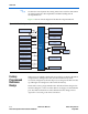
Overview f See the Nios II Development Kit, Getting Started User Guide for instructions on setting up the Nios development board and installing Nios II development tools. Figure 1–1shows a block diagram of the Nios development board. Figure 1–1. Nios Development Board, Stratix II Edition Block Diagram 16 Mbyte DDR SDRAM 50MHz Oscillator 2 Mbyte SSRAM Vccint 1.2-V 5.0 V Regulators EPCS64 Configuration Device Vccio 3.
Overview In the course of development, you might overwrite or erase the flash memory space containing the default reference design. Altera provides the flash image for the default reference design so you can return the board to its default state. Refer to Appendix A: Restoring the Factory Configuration for more information.
Overview 1–4 Reference Manual Nios Development Board Stratix II Edition Altera Corporation May 2007
2. Board Components Component List This section introduces all the important components on the Nios development board. See Figure 2–1 and Table 2–1 for component locations and brief descriptions of all board features. Figure 2–1.
Board Components Table 2–1. Nios Development Board, Stratix II Edition Components & Interfaces (Continued) Board Designation Name Description Memory U74 SSRAM memory 2 MBytes of synchronous SRAM. U5, LED7 Flash memory 16 MBytes of nonvolatile memory for use by both the FPGA and the configuration controller. LED7 lights whenever the flash chip-enable is asserted. U63 DDR SDRAM memory 32 MBytes of DDR SDRAM.
Board Components Table 2–1. Nios Development Board, Stratix II Edition Components & Interfaces (Continued) Board Designation Name Description SW9 Factory Config button Push-button switch to reconfigure the FPGA with the factory-programmed reference design. SW10 Reset, Config Push-button switch to reset the board. LED0 – LED3, LED6 Configuration status LEDs LEDs that display the current configuration status of the FPGA. Y2 Oscillator 50 MHz clock signal driven to FPGA.
Board Components The development board provides two separate methods for configuring the FPGA: f Push-Button Switches (SW0 SW3) 1. Using the Quartus® II software running on a host computer, a designer configures the device directly via an Altera download cable connected to the FPGA JTAG header (J24). 2. When power is applied to the board, a configuration controller device (U3) attempts to configure the FPGA with hardware configuration data stored in flash memory.
Board Components Individual LEDs (D0 - D7) This Nios II development board provides eight individual LEDs connected to the FPGA. Refer to “Push-Button Switches (SW0 - SW3)” on page 2–4. D0 – D7 are connected to general purpose I/O pins on the FPGA as shown in Table 2–4. When a pin drives logic 0, the corresponding LED turns on. Table 2–4.
Board Components Table 2–5. Dual Seven-Segment Display FPGA Pin U8 & U9 Pin Pin Function Board Net Name U8 L8 10 a hex_0A L9 9 b hex_0B M7 8 c hex_0C M8 5 d hex_0D M5 4 e hex_0E M6 2 f hex_0F N4 3 g hex_0G N5 7 dp hex_0DP K8 10 a hex_1A K9 9 b hex_1B U9 SSRAM Chip (U74) L4 8 c hex_1C L5 5 d hex_1D M3 4 e hex_1E M4 2 f hex_1F L6 3 g hex_1G L7 7 dp hex_1DP U74 is a 32-bit, 2 MByte Cypress SSRAM chip.
Board Components Table 2–6 shows all connections between the FPGA and the SSRAM chip. Table 2–6.
Board Components Table 2–6.
Board Components Table 2–6. SSRAM Pin Table (Continued) FPGA Pin U74 Pin Pin Function Board Net Name G18 88 GW_n ssram_gw_n A12 89 CLK sram_clk The following pins on U74 have fixed connections, which restricts the usable modes of operation: ■ ■ ■ MODE is pulled low to enable Linear Burst ZZ is pulled low to leave the chip enabled GLOBALW_n is pulled high to disable the global write.This is the default behavior for GLOBALW_n that can be changed.
Board Components Table 2–7.
Board Components Flash Memory (U5) U5 is an 8-bit, 16 MByte AMD flash memory device connected to the FPGA. The part number is S29GL128M10TFIR1. Refer to Table 2–8 for connections between the FPGA and the flash memory chip. U5 can be used for two purposes: 1. A Nios II embedded processor implemented on the FPGA can use the flash memory as general-purpose memory and non-volatile storage. 2.
Board Components Table 2–8.
Board Components Ethernet MAC/PHY (U4) & RJ45 Connector (RJ1) The LAN91C111 chip (U4) is a 10/100 Ethernet media access control and physical interface (MAC/PHY) chip. The control pins of U4 are connected to the FPGA so that Nios II systems can access Ethernet networks via the RJ-45 connector (RJ1) as shown in Figure 2–4. The Nios II development tools include hardware and software components that allow Nios II processor systems to communicate with the LAN91C111 Ethernet device. Figure 2–4.
Board Components Table 2–9.
Board Components Table 2–9.
Board Components J19 is able to transmit all RS-232 signals. Alternately, the FPGA design can use only the signals it needs, such as J19’s RXD and TXD pins. LEDs are connected to the RXD and TXD signals and visually indicate when data is being transmitted or received. Figure 6 and Table 2–10 show the pin connections between the serial connectors and the FPGA. Figure 2–5.
Board Components ■ 41 I/O pins for prototyping. All 41 I/O pins connect to user I/O pins on the FPGA. Each signal passes through analog switches to protect the FPGA from 5.0 V logic levels. These analog switches are permanently enabled. The output logic-level on the expansion prototype connector pins is 3.3 V. ● ● ■ ■ ■ ■ ■ ■ PROTO1 switches: U19, U20, U21, U22 and U25 PROTO2 switches: U27, U28, U29, U30 and U31 A buffered, zero-skew copy of the on-board oscillator output from U2.
(1) (2) (3) (4) proto1_io35 proto1_io37 proto1_io39 10 12 14 9 11 13 1 3 5 7 9 11 13 15 17 19 proto1_io34 proto1_io36 proto1_io38 (1) Vunreg NC 2–18 Reference Manual Nios Development Board Stratix II Edition VCC3_3 VCC3_3 (2) proto1_osc (3) proto1_pllclk (4) proto1_clkout VCC3_3 VCC3_3 VCC3_3 20 18 16 14 12 10 8 6 4 GND GND GND GND GND GND GND GND GND GND proto1_io33 8 7 proto1_io32 J12 2 proto1_io31 6 5 proto1_io30 VCC5 proto1_io29 2 4 1 3 GND proto1_io40 29 31 33 3
Board Components . Table 2–11.
Board Components Table 2–11.
(1) (2) (3) (4) Altera Corporation May 2007 Reference Manual 3 5 7 9 11 13 15 17 19 NC VCC3_3 VCC3_3 (2) proto2_osc (3) proto2_pllclk (4) proto2_clkout VCC3_3 VCC3_3 VCC3_3 proto2_io39 14 13 proto2_io38 20 GND GND GND GND GND GND GND GND GND 29 31 33 35 37 39 proto2_io22 proto2_io24 proto2_io25 proto2_io27 proto2_io28 19 GND proto2_io21 17 proto2_io14 27 15 proto2_io12 proto2_io19 13 proto2_io10 25 11 proto2_io8 proto2_io18 9 proto2_io6 23 7 proto2_io4 proto2_io17 5
Board Components Table 2–12.
Board Components Table 2–12.
Board Components Figure 2–10. CompactFlash Connector Most pins of CON3 connect to I/O pins on the FPGA. The following pins have special connections: ■ Pin 13 and 38 of CON3 (VCC) are driven by a power MOSFET that is controlled by an FPGA I/O pin. These connections allow the FPGA to control power to the CompactFlash card for the IDE connection mode. Pin 26 of CON3 (-CD1) is pulled up to 5 V through a 10 kΩ resistor.
Board Components Table 2–13.
Board Components Table 2–13. CompactFlash Pin Table (Continued) FPGA Pin CON3 Pin Pin Function Board Net Name (1) H8 43 INPACK_n proto1_io39 J7 44 REG_n proto1_io40 AE7 32 CS1_n cf_cs_n AE8 9 ATA_SEL_n cf_atasel_n AB12 5 Power supply enable cf_power (2) AB11 26 CD1_n cf_present_n 57 (U3) 41 RESET# proto1_RESET_n (3) Notes to Table 2–13: (1) (2) (3) f PMC Connector (JH1 & JH2) Nets proto_io16, proto_io20, and proto_io21 do not connect to CON3.
Board Components Figure 2–11. PMC Connector Pin 1 Pin 1 JH1 JH2 The PMC connector supplies +3.3 V, +5.0 V and ±12. V, as required by the PCI specification. However, DC power regulators for these supplies cannot provide enough power to fully satisfy the PCI power specification. The current that the board can supply through JH1 and JH2 is dependent on the design configured in the FPGA.
Board Components Table 2–15 lists the connections between the PMC connector and the FPGA. Table 2–15.
Board Components Table 2–15.
Board Components f For details on Nios II debugging products that use the Mictor connector, see www.altera.com. Figure 2–12 shows an example of an in-target system analyzer ISANios/T by First Silicon Solutions (FS2) Inc. connected to the Mictor connector. For details, see www.fs2.com. Figure 2–12. An ISA-Nios/T Connecting to the Mictor Connector (J25) J25 Five of the signals connect to both the JTAG pins on the FPGA (U60), and the FPGA’s JTAG connector (J24).
Board Components Table 2–16 shows the pin out information for J25. Table 2–16.
Board Components Table 2–17 lists the connections between the FPGA, U3, and the test points. Table 2–17. Test Point Pin Table Test Point EPCS64 Serial Configuration Device (U69) FPGA Pin CPLD Pin 75 Board Net Name TP1 V18 pld_user0 TP2 AC19 76 pld_user1 TP3 W16 77 pld_user2 TP4 W17 78 pld_user3 TP5 AE17 79 pld_user4 TP6 AE18 80 pld_user5 TP7 AE20 81 pld_user6 TP8 AE21 83 pld_user7 U69 is a serial configuration device connected to the FPGA.
Board Components 1 f Configuration Controller Device (U3) The orientation of J27 is the reverse of J24. See the Serial Configuration Devices chapter in Altera's Configuration Device Handbook for more information about the EPCS64 device. See the EPCS Device Controller Core with Avalon Interface chapter in the Quartus II Handbook, Volume 5: Altera Embedded Peripherals for information about the EPCS serial flash controller component in SOPC Builder.
Board Components Table 2–19. Configuration Status LED Indicators LED Led Name Color Description LED3 Loading Green This LED blinks while the configuration controller is actively transferring data from flash memory into the FPGA. LED4 Error Red If this LED is on, then configuration was not transferred from flash memory into the FPGA. This can happen if, for example, the flash memory does not contain either a valid user or factory configuration.
Board Components Figure 2–15. CPU Reset Button SW8 CPU Reset SW9 – Factory Config Pressing Factory Config (SW9) commands the configuration controller to reconfigure the FPGA with the factory configuration. Refer to Figure 2–16. Figure 2–16. Factory Config Button SW9 Factory Config SW10 – Reset, Config Reset, Config (SW10) is the power-on reset button. Refer to Figure 2–17. When SW10 is pressed, a logic 0 is driven to the power on reset controller (U18).
Board Components Figure 2–17.
Board Components Nios II reference design is factory-programmed into the factory configuration region of the flash memory. In addition, the FPGA can be configured by the EPCS64 serial configuration device. Configuration Process At power-up or reset, the configuration controller attempts to configure the FPGA with data from one of three sources, in the following order: 1. The EPCS64 serial configuration device 2. The user configuration from flash memory 3.
Board Components Flash Memory Partitions The configuration controller expects user and factory configuration data to be stored at fixed locations (offsets) in flash memory. In addition, the factory-programmed reference design expects Nios II software and data to exist at certain locations in flash memory. Table 2–20 shows the expected flash memory partitioning. Table 2–20.
Board Components User Configuration The user configuration partition is 4 MB, starting at offset 0x00800000. This section contains the FPGA configuration data for the user configuration. Nios II development tools include documentation on how to create your own user configuration image and program it into flash memory. Factory Configuration The factory configuration partition is 4032 KB, starting at offset 0x00C00000. This section contains the FPGA configuration data for the factory configuration.
Board Components Figure 2–18. JTAG Connector (J24) to Stratix II Device To Mictor Connector (J25) JTAG Signals FPGA (U62) JTAG Connector (J24) TDI TMS TCK TDO TRST Figure 2–19. USB Blaster Connected to J24 JTAG Connector Pin 1 J24 The FPGA’s JTAG pins can also be accessed via the Mictor connector (J25). The pins of J24 are connected directly to pins on J25, and care must be taken so that signal contention does not occur between the two connectors.
Board Components JTAG Connector to EPM7256AE Device (J5) J5 connects to the JTAG pins (TCK, TDI, TDO, TMS, TRST) of the EPM7256AE device (U3). Altera Quartus II software can perform insystem programming (ISP) to reprogram the EPM7256AE device (U3) with a new hardware image via an Altera download cable as shown in Figure 2–20. 1 The orientation of J5 is rotated 180 degrees compared to J24. Most users never need to reprogram the configuration controller design in the EMP7256AE device.
Board Components Figure 2–21. Clock Circuitry osc_CLK3 osc_CLK2 DDR SDRAM (U63) osc_CLK0 osc_CLK1 sram_CLK SSRAM (U74) sram_CLKIN sdram_CLKIN Oscil ator (Y2) SMA External Input (J4) Clock Buffer (U2) mictor_CLK FPGA (U62) PLLs PMC_CLK Mictor (J25) PMC (JH1 & JH2) proto1_PLLCLK proto1_CLKOUT PROTO1 proto1_OSCCLK proto2_PLLCLK proto2_CLKOUT PROTO2 proto2_OSCCLK cpld_CLKOSC MAX (U3) Note to Figure 2–21: (1) To use an external clock signal, remove the crystal oscillator from its socket.
Board Components The FPGA receives clock input from buffer U2, and from the PROTO1 and PROTO2 connectors, as shown in Table 2–21. Table 2–21.
Board Components Power-Supply Circuitry The Nios development board runs on a 16.0 V, unregulated, input power supply connected to J26. On-board circuitry generates ±12.0 V, +5.0 V, +3.3 V, +2.5 V, and +1.2 V regulated power levels. For applications requiring high current, separate voltage levels can be supplied from a workbench power supply. ■ ■ ■ ■ ■ ■ The input power-supply on J26 can be either center-negative or center-positive.
Appendix A. Restoring the Factory Configuration Introduction To restore the factory configuration, you must reprogram the flash memory on the board, and you must reprogram the EPM7256AE configuration controller device. Nios II Embedded Design Suite provides the files required for this operation in the directory /examples /factory_recovery. Reprogramming the Flash Memory To reprogram the flash memory on the development board, perform the following steps: 1.
2. Launch the Quartus II software, and click Programmer on the Tools menu. 3. Click Add File and select the following programming file: /examples/ factory_recovery/niosII_stratixII_2s60_rohs/config_controller.pof. 4. In the Programmer, turn on the Program/Configure checkbox, and click Start to reprogram the EPM7256AE device. 5. Press the Factory Config button to perform a power on reset and reconfigure the FPGA from flash memory.
Appendix B. Connecting to the Board via Ethernet Introduction The Nios development board is factory-programmed with a reference design that implements a web server, among other functions as shown in Figure B–1. This chapter describes how to connect a host computer to the board's Ethernet port, assign an IP address to the board, and browse to the web server from the host computer. Figure B–1.
2. Point-to-Point Connection — To use your Nios development board connected directly to a host computer point-to-point (not on a LAN), do the following: a. Connect one end of your RJ45 cable to the female socket in the crossover adapter and insert the male end of the crossover adapter into RJ1 on the Nios development board as shown in Figure B–2. Figure B–2. Point-to-Point Connection RJ1 b. Connect the other end of the RJ45 connector directly to the network (Ethernet) port on your host computer.
LAN Connection If you have connected your board to a LAN, the board will either obtain a dynamic IP address using DHCP, or a static IP address stored in flash memory. If you do not know whether or not your LAN supports DHCP, it is easiest to try DHCP first. DHCP Upon reset, the web server attempts to acquire an IP address via the DHCP protocol. The board continues to attempt DHCP self-configuration for two minutes.
5. Press the ! key to abort the DHCP process and display a prompt. If you don't abort the DHCP process, it will fail after two minutes, and eventually a prompt will appear. 1 6. The monitor's prompt is the + character. You can enter h at the prompt for a complete list of supported commands. At the prompt, type xip: The xip command saves the IP address in flash memory. In general, you only need to assign an IP address to your board once.
modifying the host computer's IP address, your computer is ready to connect to the web server. Refer to “Browsing to Your Board” on page B–5 to continue. If you don't have the ability to change the IP address of your host computer, you can change the IP address of the board to match the subnet of the host computer. For example, if your computer's IP address is 1.2.3.4, then you can assign the address 1.2.3.5 to your board. To change the board IP address, follow the steps in “Static IP Address ” on page B–3.
B–6 Reference Manual Nios Development Board Stratix II Edition Altera Corporation May 2007