Nios II System Architect Design Tutorial 101 Innovation Drive San Jose, CA 95134 www.altera.com TU-01004-1.
Copyright © 2009 Altera Corporation. All rights reserved. Altera, The Programmable Solutions Company, the stylized Altera logo, specific device designations, and all other words and logos that are identified as trademarks and/or service marks are, unless noted otherwise, the trademarks and service marks of Altera Corporation in the U.S. and other countries. All other product or service names are the property of their respective holders. Altera products are protected under numerous U.S.
Contents Chapter 1. Getting Started Tutorial Introduction . . . . . . . . . . . . . . . . . . . . . . . . . . . . . . . . . . . . . . . . . . . . . . . . . . . . . . . . . . . . . . . . . . . . 1–1 Hardware and Software Requirements . . . . . . . . . . . . . . . . . . . . . . . . . . . . . . . . . . . . . . . . . . . . . . . . . . . . . 1–1 Acquire the NEEK . . . . . . . . . . . . . . . . . . . . . . . . . . . . . . . . . . . . . . . . . . . . . . . . . . . . . . . . . . . . . . . . . . . .
iv Contents Additional Information Taking the Next Step . . . . . . . . . . . . . . . . . . . . . . . . . . . . . . . . . . . . . . . . . . . . . . . . . . . . . . . . . . . . . . . . . . How to Contact Altera . . . . . . . . . . . . . . . . . . . . . . . . . . . . . . . . . . . . . . . . . . . . . . . . . . . . . . . . . . . . . . . . Revision History . . . . . . . . . . . . . . . . . . . . . . . . . . . . . . . . . . . . . . . . . . . . . . . . . . . . . . . . . . . . . . . . . . . . .
1. Getting Started Tutorial Introduction This tutorial teaches you how to use SOPC Builder, the Quartus® II software, and the Nios® II Embedded Design Suite (EDS) to implement a digital picture viewer in a Cyclone III FPGA. In this tutorial, you build a processor-based hardware system in programmable logic for the Nios II Embedded Evaluation Kit, Cyclone® III Edition (NEEK) and run software on it.
1–2 Chapter 1: Getting Started Hardware and Software Requirements Install the Design Software This section teaches you how to install the Quartus II software v9.0 and the Nios II EDS v9.0. The design software is available on the Altera Complete Design Suite DVD or by downloading from the web. Two installation options are available for the Altera Complete Design Suite, a subscription package and a free package.
2. Designing the System Introduction To architect a system, you specify the design requirements and develop a suitable design strategy to address each requirement. Design requirements include immediate design goals of the product and features to keep your product commercially successful in the future. You must consider desired application functionality, cost, flexibility to add future features, time to market, and obsolescence.
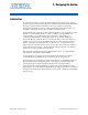
2–2 Chapter 2: Designing the System Design Flow Design Flow Figure 2–1 depicts the typical flow for embedded system design. Figure 2–1.
Chapter 2: Designing the System Design Requirements 2–3 In this tutorial you perform the following steps: 1. Build an SOPC system: a. Open the Quartus II project. b. Start SOPC Builder c. Select and configure system components, including IP MegaCore functions d. Make connections e. Assign clocks and set base addresses f. Set interrupt and arbitration priorities 2.
2–4 Chapter 2: Designing the System Design Strategy Design Strategy SOPC Builder provides a menu of standard hardware components that you can add to your system. You can add several instances of each component. The only restriction is the resources available on your board to implement all of the components you instantiate in your design. The NEEK comprises a Cyclone III FPGA Starter Board and an LCD Multimedia High Speed Mezzanine Card (HSMC) daughtercard in addition to accessories and software.
Chapter 2: Designing the System Design Strategy 2–5 Table 2–1. Standard Hardware Components to Implement the Digital Picture Viewer Requirements Design Requirement Design Strategy Display JPEG pictures on the LCD Display 1. LCD screen controller Scroll through JPEG pictures Components Needed 1. PIO 2. A video pipeline to send video data to the LCD screen 2. Video pipeline peripherals 1. An interrupt to capture touch screen events 1. PIO 2. SPI 2. Touch screen control Frame buffering 1.
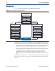
2–6 Chapter 2: Designing the System Block Diagram Block Diagram Figure 2–2 shows a high-level block diagram of the system you develop to implement the design. Figure 2–2.
3. Building the SOPC System In this chapter you add standard and custom components to the system, make connections where required, assign the clocks, set arbitration priorities, and generate the system. The tutorial SOPC Builder system contains 24 components. You start with a partially completed SOPC Builder system, to which you add a Nios II embedded processor, a DDR SDRAM high-performance controller, an Avalon-MM clock-crossing bridge peripheral, and a scatter-gather DMA controller.
3–2 Chapter 3: Building the SOPC System Specify the SOPC Builder System Components Table 3–1 shows the components in the partial system provided in your Quartus II project. Table 3–1.
Chapter 3: Building the SOPC System Specify the SOPC Builder System Components 3–3 2. Add a DDR SDRAM High Performance Controller 3. Add a Clock-Crossing Bridge Between the CPU and DDR SDRAM Clock Domains 4. Add a Scatter-Gather DMA Controller 1 Altera recommends that you save your work after you add each component. To save the current SOPC Builder system, on the File menu, click Save.
3–4 Chapter 3: Building the SOPC System Specify the SOPC Builder System Components Add a DDR SDRAM High Performance Controller Your system requires a high-performance memory block to act as a video frame buffer. To add a high-performance DDR SDRAM controller to your system, perform the following steps: 1. Under System Contents, expand Memories and Memory Controllers, expand SDRAM, and double-click DDR SDRAM High Performance Controller. 2.
Chapter 3: Building the SOPC System Specify the SOPC Builder System Components 3–5 9. Now you must remove two connections between the cpu and ddr_sdram components that are created by default. The cpu/instruction_master port and cpu/data_master port should not be connected to the ddr_sdram/s1 slave port, because the Nios II processor and the DDR SDRAM are in different clock regions.
3–6 Chapter 3: Building the SOPC System Specify the SOPC Builder System Components Figure 3–4. Avalon-MM Clock Crossing Bridge Component Settings 3. Click Finish. 4. In the Module Name column, right-click the Avalon-MM Clock Crossing Bridge component’s name, click Rename, and rename the new component cpu_ddr_clock_bridge. 5. In the Connections column, ensure that the cpu_ddr_clock-bridge/m1 master port is connected to the ddr_sdram/s1 slave port.
Chapter 3: Building the SOPC System Specify the SOPC Builder System Components 3–7 Add a Scatter-Gather DMA Controller The scatter-gather DMA controller fetches data from the video frame buffer on the DDR SDRAM and sends the data to the video pipeline. To add a Scatter-Gather DMA Controller to your system, perform the following steps: 1. Under System Contents, expand Memories and Memory Controllers, expand DMA, and double-click Scatter-Gather DMA Controller. 2.
3–8 Chapter 3: Building the SOPC System Specify the SOPC Builder System Components Table 3–2. SGDMA Component Connections From To Description lcd_sgdma/csr cpu_ddr_clock_bridge/m1 Because the Nios II processor and the SGDMA component are in different clock domains, the lcd_sgdma/csr port must connect to the clock-crossing bridge. In “Coordinate Components in the System”, you set the SGDMA component to use the same clock as the DDR SDRAM.
Chapter 3: Building the SOPC System Coordinate Components in the System 3–9 Coordinate Components in the System This section teaches you how to coordinate the components in your SOPC Builder system to ensure they work together correctly. It contains the instructions that show you how to perform the following actions: 1. Specify External Clocks and Clock Connections 2. Reassign Component Base Addresses to Eliminate Memory Conflicts 3. Set Interrupt Priorities 4. Set Arbitration Priorities 5.
3–10 Chapter 3: Building the SOPC System Coordinate Components in the System Figure 3–8. Clocks for Digital Picture Viewer SOPC Builder System 9. If the clock ports for the components do not appear in the Module Name column, perform the following steps: a. Click the Filters button below your system display. b. In the Filters dialog box, under Filter, select All. c. Close the Filters dialog box. 10.
Chapter 3: Building the SOPC System Coordinate Components in the System 3–11 Reassign Component Base Addresses to Eliminate Memory Conflicts To reassign component base addresses to eliminate undesired overlap between the address spaces of different components, perform the following steps: 1. On the System menu, click Auto-Assign Base Addresses. The tool assigns appropriate base addresses for the components. 2.
3–12 Chapter 3: Building the SOPC System Coordinate Components in the System 2. Type the interrupt priority value from Table 3–4. Figure 3–10 shows the lcd_sgdma component after you perform this step. Table 3–4.
Chapter 3: Building the SOPC System Coordinate Components in the System 3–13 Figure 3–11. Arbitration Priorities in Digital Picture Viewer SOPC Builder System 3. To hide the arbitration priorities, on the View menu, click Show Arbitration. Specify the Nios II Processor Boot Configuration Immediately after it completes its hardware reset sequence, the Nios II processor begins executing software located at a predefined memory location. The reset vector specifies this location.
3–14 Chapter 3: Building the SOPC System Coordinate Components in the System Figure 3–12. Nios II Processor Reset and Exception Vector Settings 6. Click Finish. Your SOPC Builder system content is complete and you can now generate the SOPC Builder system.
Chapter 3: Building the SOPC System Generate the System 3–15 Figure 3–13 shows your final SOPC Builder system. Figure 3–13. Final Digital Picture Viewer SOPC Builder System Generate the System After you verify that all the component names in your SOPC Builder system match the component names in Figure 3–13, you are ready to generate your system. To generate your system, on the System Generation tab, click the Generate button.
3–16 Chapter 3: Building the SOPC System Generate the System ■ System description used by the software development tool, the Nios II IDE, to build the software project After your system generates successfully, the following message appears: System generation was successful.
4. Completing the Quartus II Project In this chapter you complete the Quartus II project by adding the generated SOPC Builder system to the top-level project and adding timing constraint files to your project. You compile your project in the Quartus II software to perform analysis, synthesis, fitting, place-and-route, and timing analysis. Compilation generates an FPGA image as an SRAM object file (.sof).
4–2 Chapter 4: Completing the Quartus II Project Complete the Quartus II Project Figure 4–1. NEEK Embedded Tutorial Project Top-Level Block Diagram The Block Design file (.bdf) includes the pins required by the design, a PLL, a MUX, and some glue logic, but does not include the logic in the SOPC Builder system. You must add the SOPC Builder system as a new logic block to the schematic design.
Chapter 4: Completing the Quartus II Project Complete the Quartus II Project 4–3 Figure 4–2. SOPC Builder System Inserted in Top-Level Project 5. On the File menu, click Save Project to save the top-level schematic with the SOPC Builder system. Add Timing Constraints and Compile Your Design To ensure the design works correctly, you must add explicit timing constraints to the project. For this tutorial, the timing constraints are available in two files, neek_hw_lab.sdc and ddr_sdram_phy_ddr_timing.sdc.
4–4 Chapter 4: Completing the Quartus II Project Configure the FPGA 7. Use the Up and Down buttons as necessary to ensure the sequence of the files is correct. This step is necessary to ensure the constraints are applied in the correct order. Figure 4–3 shows the required file order. Figure 4–3. Settings Dialog Box After Two New Timing Constraint Files Added to Project 8. Click OK. The design is ready for compilation. 9. To compile your design, on the Processing menu, click Start Compilation.
Chapter 4: Completing the Quartus II Project Configure the FPGA 4–5 2. Ensure that the power switch (SW1) on the back side of the NEEK is in the OFF position (up). 3. Connect the USB cable from your PC to the NEEK. 4. Connect the power cable to the NEEK. 5. Press the power switch to turn on the NEEK. 6. In the Quartus II Programmer, click Hardware Setup. 7. Under Currently selected hardware, click USB-Blaster [USB-0]. 8. Click Close. 9. Click Auto Detect.
4–6 Chapter 4: Completing the Quartus II Project Configure the FPGA After you complete all the steps in this chapter, you have successfully compiled and downloaded the FPGA image to the Cyclone III device on your NEEK. The processor is ready to run. Next, you must develop the software application and download it to the NEEK.
5. Creating the Software Application In this chapter you use the Nios II IDE to develop the software application that runs on your system. You create a new software application project, add the software source files to the project, configure the project, and build it. The result of the build process is an executable and linkable file (.elf). The Nios II IDE downloads the application .elf to the memory location at which the Nios II processor expects to find the executable image.
5–2 Chapter 5: Creating the Software Application Create a New Software Project in the Nios II IDE Figure 5–1 shows the New Project dialog box after you perform these steps. Figure 5–1. New Project Wizard Settings for Tutorial Software Application Project 8. Click Next. 9. Turn on Create a new system library. 10. Click Finish. 11. If you are prompted to open the Nios II C/C++ perspective, click Yes.
Chapter 5: Creating the Software Application Add Source Code Files to the Project 5–3 Because this software project is based on the blank template, the project directories do not yet contain any source code files. Add Source Code Files to the Project Your working directory contains a software_source_files folder. The files in this folder are the source code files for the tutorial software application project. To copy these files to the software application folder, perform the following steps: 1.
5–4 Chapter 5: Creating the Software Application Specify the Zip File System Settings Figure 5–4. System Library Settings for Digital Picture Viewer The software design uses the MicroC/OS-II operating system. All stdout, stdin, and stderr messages are directed to the jtag_uart. You use the auto-generated linker script to store the heap linker section in DDR SDRAM memory and the other linker sections—program memory, read-only data memory, read/write data memory, and stack—in SSRAM memory. 5. Click Apply.
Chapter 5: Creating the Software Application Build the Software Project 5–5 7. Click Altera Zip Read-Only File System. 8. Turn on Add this software component. 9. Under Offset, type 0x400000. 10. Click Browse. 11. Click jpeg_images.zip. 12. Click OK. Figure 5–5. Altera Read-Only Zip File System Settings for Digital Picture Viewer 13. Click OK. 14. Click OK.
5–6 Chapter 5: Creating the Software Application Program the Zip File to Flash Memory To program the flash memory with the .flash you created in the build process, perform the following steps: 1. In the Nios II IDE, on the Tools menu, click Flash Programmer. 2. Click the New icon to create a new configuration. Figure 5–6 shows the New icon. Figure 5–6. Flash Programmer Settings to Program Flash Memory With JPEG Images .zip File New Icon 3. Turn on Program a file into flash memory. 4.
Chapter 5: Creating the Software Application Run the Software Application on the NEEK 5–7 Run the Software Application on the NEEK Running an application on the target hardware requires the following two image files: ■ FPGA hardware image SRAM Object File (.sof) ■ Software executable image (.elf) In Chapter 4, Completing the Quartus II Project, you configured the FPGA by downloading the .sof to the FPGA. After you configure the FPGA, it is ready to run the software application.
5–8 Chapter 5: Creating the Software Application Interact with the Software Application Figure 5–7. Output from Successful Run of Digital Picture Viewer Interact with the Software Application When the neek_picture_viewer application starts running on the Nios II processor, the digital picture viewer displays the first JPEG image. To display the next image, press the Forward button on the LCD touch screen. To display the previous image, press the Back button on the LCD touch screen.
Additional Information Taking the Next Step Altera offers many resources to help you get started designing your own embedded designs. If you are starting from scratch, Altera recommends that you purchase a Nios II development kit. Each kit includes pre-generated Nios II processor systems and a Nios II IP license. If you already have a working project, you can add an SOPC Builder system to your top-level project as a stub or add your design to the SOPC Builder system as a custom component.
Info–2 How to Contact Altera Subject Information Source Online tutorials and in-person training Embedded Hardware Designer Training SOPC Builder Volume 4: SOPC Builder of the Quartus II Handbook Embedded Software Designer Training How to Contact Altera For the most up-to-date information about Altera products, refer to the following table. Contact (Note 1) Contact Method Address Technical support Website www.altera.com/support Technical training Website www.altera.
Info–3 Typographic Conventions Visual Cue Meaning “Subheading Title” Quotation marks indicate references to sections within a document and titles of Quartus II Help topics. For example, “Typographic Conventions”. Courier type Indicates signal, port, register, bit, block, and primitive names. For example, data1, tdi, and input. Active-low signals are denoted by suffix n. For example, resetn. Indicates command line commands and anything that must be typed exactly as it appears.
Info–4 Typographic Conventions Nios II System Architect Design Tutorial © June 2009 Altera Corporation Preliminary