FrameWork Logic Users Guide Innovative Integration Copyright 2005. All rights reserved. All information in this document is property of Innovative Integration and all rights are reserved. This information is provided solely for the purpose of supporting use of Innovative Integration products and software. No further license is granted or implied by this publication. Revision 1.0 Changes Initial release.
1 Table of Contents Table of Contents 1 Table of Contents.............................................................................................................2 2 List of Figures.................................................................................................................. 4 3 List of Tables.................................................................................................................. 6 4 Introduction...............................................................
6.1.4.6 DSP Interface.......................................................................................... 55 6.1.4.6.1 DSP Bus EMIF A............................................................................55 6.1.4.6.2 DSP Bus EMIF B............................................................................ 59 6.1.4.7 Event Log................................................................................................59 6.1.5 MATLAB Simulink Logic Examples......................................
2 List of Figures Illustration Index Illustration 1: VHDL Development Process...................................................................... 10 Illustration 2: Logic Architecture Showing Hardware and Application Layers.................11 Illustration 3: Compiling the Simulation Libraries............................................................ 13 Illustration 4: Setting Simulation Library Compilation Properties....................................
Illustration 40: ChipScope Core Declarations................................................................... 43 Illustration 41: ChipScope Core Instantiation....................................................................44 Illustration 42: Xilinx ChipScope in Use...........................................................................45 Illustration 43: Quixote Logic and Peripherals.................................................................. 47 Illustration 44: Quixote Logic Block Diagram...
3 List of Tables Index of Tables Table 1: Document Revision History...................................................................................1 Table 2: Supported Logic Development Tools.................................................................... 7 Table 3: Logic Environments Pros and Cons.......................................................................9 Table 4: Xilinx Report Files Generated During Implemention.........................................
4 Introduction This manual is written to assist in the creation, implementation and testing of custom logic for Innovative Integration products. The scope of this manual is limited to discussion of the logic development tools, example logic designs and logic libraries provided in the Framework Logic toolset. Additional documentation on each product is provided for hardware features and software in other manuals. These are used in conjunction with this manual for product development and use.
Logic development and are discussed in this manual. If you are using other tools, they should have similar capabilities. 4.2 Organization of this Manual This manual covers the main topics in using the Framework Logic for Innovative Integration products for both HDL and MATLab Simulink development methods. The first few sections describe the HDL tools and development methods including synthesis, placement and routing, and simulation.
5 Logic Development Process The FrameWork Logic system supports two logic development methods: VHDL, or MATLab Simulink, or a combination. Each system offers benefits and have strengths that in some cases complement each other. VHDL development is very flexible, allowing the developer the full freedom of a high level language that is expressive and extensible.
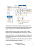
Illustration 1: VHDL Development Process The application development begins with the FrameWork Logic code for the product you are using. In many cases, the example application code provides a good starting point for your application logic. In most cases the application logic shows a basic data flow between the IO devices, such as A/D and D/A converters, to the logic and DSP or system.
Illustration 2: Logic Architecture Showing Hardware and Application Layers Hardware Interface Layer HW Interface Application Layer (your logic does here) HW Interface Code for your application layer design can be created in a number of ways: written in VHDL or Verilog, created in MATLAB, or included as a black box netlist from a third party such as Xilinx or others. If you design you logic to run on a single clock it is then easier to integrate into the application layer of the FrameWork Logic.
5.1.2 VHDL Simulation Simulation is an important part of the logic development process. All designs that are targeted at using the large logic devices supported by the Framework Logic require simulation for successful implementation. If you do not simulate your design, it is unlikely that you will successfully complete it during your lifetime. For simulation, we are currently supporting ModelSim 6.1 PE.
Selecting the device Compiling the libraries Illustration 3: Compiling the Simulation Libraries Illustration 4: Setting Simulation Library Compilation Properties Simulation can be started in either the Xilinx ISE environment, or by using the ModelSim tool in a standalone mode. In Xilinx ISE, select the test bench file in the Sources in Project window. This then will show the simulations that can be run in the Processes window using ModelSim.
When you enter the ModelSim tool from Xilinx ISE, it will execute a default macro that compiles the files and begins the simulation. If you enter in standalone mode, you will need to compile the files within the ModelSim. Select test bench file here Select ModelSim here Illustration 5: Invoking ModelSim from Xilinx ISE In many cases a macro file is provided that compiles the files within ModelSim according to the macro file order.
Illustration 6: Configuring Xilinx ISE to use a custom DO file Innovative Integration FrameWork Logic User Guide 15
Illustration 7: Loading the simulation in ModelSim When the design is loading, you will see each components loaded in the transaction window as shown here. If anything fails to load, check that its ports match those in the instance where it was used.
Illustration 8: Example ModelSim Workspace After Loading Once the design is loaded, the design hierarchy is shown in the Workspace window with the test bench at the top of the hierarchy. Here is an example.
Illustration 9: ModelSim Wave Window Example Once you are inside the ModelSim environment, you should be able to use the tools to run simulations of the design. The wave window is many times the main focus since it gives a logic analyzer view of the design. You can quickly view debug the design within ModelSim because you can probe the logic down to the lowest level.
5.2 Logic Development using MATLAB Simulink MATLab Simulink provides a powerful method of developing logic using a high level design tool that integrates hardware into the MATLAB Simulink environment. Complex signal processing designs can be developed rapidly using the Simulink block diagrams interacting with the actual hardware in real time.
5.2.1 Installation You must have installed MATLAB Simulink prior to installing the product MATLAB support. The co-simulation library is provided as a zip file and a Matlab installation script. setup_<>.zip Unzip the software, preserving the directory structure. The next step is to start Matlab and point at the installation directory In this directory, you will find a Matlab installation script, <>_compilation.m .
Illustration 13: Matlab Installation Directory Example 4. Quit MATLAB and restart.. Now the product library should be visible in the Simulink Library Browser window. Illustration 14: Simulink Product Library Example The library is now ready for use in MATLAB. The files controlling the compilation process are in the C:\MATLAB7\toolbox\sysgen\jtagcosim\product_name directory.
5.2.2 MATLAB Simulink Use In MATLAB, you can make new block diagrams for logic designs using the libraries for Xilinx and the specific product. Creating a new logic diagram is often aided by starting with one of the examples for the product you are using as a starting point. You can then drag and drop Simulink blocks into the worksheet to build the logic functionality you need.
An important feature in the Simulink environment is the ability to use Simulink for active cosimulation. This means that real hardware can be accessed from within in the Simulink environment. You can generate test signals, run them through the logic device on you card and then observe the output. This allows you develop on the real hardware for design, test and debug. Gateways are used to provide the link between the Simulink environment and the hardware.
SRAM used for data capture or playback Illustration 17: Example of Real-time Signal Capture in MATLAB To get signals from MATLAB into the hardware, the SRAM can be used as an arbitrary waveform generator when it is loaded with a test waveform that is then played out real-time. MATLAB is ideal for generation of the complex waveforms found in communications applications.
5.3 Making the Physical Logic After the logic has been created, either with HDL or MATLAB, it must be implemented in the logic through a process of placing and routing the logic into the physical device. For either development process, the physical design is done using the Xilinx tools. These tools take the netlist created by the synthesis process or Xilinx System Generator and map it into the physical device while meeting timing and physical constraints.
process. Double-clicking the icon allows you to configure the Xilinx ISE tools that are used for the logic build just as you would for an HDL design. The implementation settings are set in the window as shown here. Illustration 20: Xilinx System Generator Implementation Control 5.3.1 Place and Route Reports The place and route implementation by the Xilinx tools results in several files you may want to review in case of problems.
File extension Contents What to Look For .BLD The output from the NGDBuild process that link all the logic together There should be no errors. This program issues numerous warnings but there should be no errors. Most link errors occur because of missing netlist files – Coregen put the files somewhere else, or a missing netlist from a black box. .MAP The output from the MAP process that does the logic mapping to the physical device. Removes unused logic and.
The Xilinx IMPACT application is used to load the logic into the application FPGA. The IMPACT tool may be invoked from the Xilinx ISE tool or as a standalone application. When you enter the tool, you will be prompted for either a stored project or to create a new one. The first time you use this, you should create a new project. Later, you can save the project and it remembers the scan chain and files for the project.
The next screen will prompt for what type of configuration to perform. Choose the Boundary Scan Mode as shown. Illustration 23: Choosing the Boundary Scan Mode for IMPACT Next, IMPACT will prompt for the JTAG chain identification. Choose the automatic identify mode.
If all goes well, IMPACT will find all the devices in the JTAG chain and display them as shown in this example. If not, check the cable connection to the board. The cable should be detected by IMPACT; if not, check that the port it is connected to on the PC is working and in the proper mode. If the chip is not detected, be sure you have the right scan path, that the board is powered up normally, and that IMPACT was able to connect to the scan path.
Illustration 26: Programming Devices using JTAG under IMPACT 5.4.2 Loading the Logic Using PROM Images 5.4.2.1 Making the Device Image For all Innovative products, an EXORMacs format (.EXO) text file must be generated from the output .BIT file produced by the place and route process. This is done by opening the Xilinx IMPACT tool that is a PROM File Formatter utility from within the ISE and converting the BIT file into an EXO file.
Illustration 27: Using IMPACT to Make a PROM Image The next screen will prompt you to either configure devices or make a configuration file. To make a PROM image, select Prepare Configuration Files.
For a generic PROM file, used for most Innovative products, on the next screen you should select PROM file for the image type. Illustration 29: Selecting the Configuration Method in IMPACT The PROM properties must be set to “bytewide” and EXORmacs to generate the required EXO file. Once the properties are set, the .EXO file is generated in the source directory.
Illustration 30: Selecting the PROM size in IMPACT In PROM Configuration screen, select the following options: • Select Parallel PROM. • Select EXO as File Format. • Memory Fill Value - 0xFF then provide a File Name.
Illustration 31: Selecting the BIT file in IMPACT You will then be prompted before the file is made – you last chance to not overwrite you last PROM if you did not change the name or file path.
Illustration 32: Ready to Make the PROM Image in IMPACT The final screen will report successful operation.
You are now ready to load the PROM image using one of the tools provided by Innovative or by your application. Each family of cards has a specific logic programming utility and software support. Here is a list of the tools for the card families.
5.4.2.2 Velocia Download The Velocia family of products, including Quixote and Quadia, use a simple Windows application to download logic images to the card. The same application can be used to load DSP files, see the software documentation for information. Note: The application logic must be loaded after each power-up since there is no on-card logic ROM. The logic is loaded over the SelectMAP interface to the FPGA via the PCI bus. The logic may be loaded and reloaded at any time during operation.
also. These are detailed in the software manual. 5.5 Debugging It is inevitable that the logic will require some debugging and it is best to have a strategy for debug before you actually use the hardware. Debugging on actual hardware is difficult because you have poor visibility into the FPGA internals. For HDL designs, the best and easiest debug method is simulation for functional and timing problems. This gives the best visibility and interactivity to debug problems before the real hardware is tested.
Another built-in test method is to use data checkers in the logic sprinkled through the data chain help to spot the source of problems. If you have a missing timing constraint or a clock domain issue, these can be hard to catch since they may be rare. A data checker gives you a way to look for bad data and then trigger ChipScope or the logic analyzer. In many cases, rare errors are impossible to catch without this sort of data checker.
to pre-trigger or post-trigger in the software which makes trigger design easier. Here is one of the common cables used for debug, just for reference. Illustration 37: Xilinx Parallel IV Cable for Debug and Development Illustration 38: Xilinx Parallel Cable IV Target Cable Illustration 39: Xilinx Parallel Cable IV Pinout on IDC 5x2 2MM Header CAUTION: The user MUST make sure that Xilinx JTAG cable connector is plugged in the proper polarity to the Innovative target connector.
5.5.2.1 Declaration Of ChipScope Core in VHDL The ChipScope core is simple to use. Just connect up the signal for observation to the data ports, the trigger signals to trigger and the clock. The number of ports and triggers is defined when you create the debug core in the ChipScope tool. The clock is used as the sample clock for the logic analyzer, so you must use a clock that is higher frequency than the signals you wish to observe. Here’s a core we used in debug shown below.
--- ICON core component declaration -------------------------------------------------------------------component icon port ( control0 : out std_logic_vector(35 downto 0) ); end component; --------------------------------------------------------------------- ICON core signal declarations -------------------------------------------------------------------signal control0 : std_logic_vector(35 downto 0); ---------------------------------------------------------------------------------------------------
--------------------------------------------------------------------- ICON core instance -------------------------------------------------------------------i_icon : icon port map ( control0 => control0 ); --------------------------------------------------------------------- ILA core instance -------------------------------------------------------------------i_ila : ila port map ( control => control, clk => clk, data => data, trig0 => trig0 ); control <= control0; trig0(0) <= sw_trigger(2)or sw
In this case, the designer was using the DSP EMIF A clock as the ChipScope core clock and had several triggers including DSP memory decodes and software triggers. Some of the signals being observed are shown as well such as FIFO read enables and so forth. Looks like the debug was for some type of DSP access problem. Once the core is in the design, you can then trigger on different conditions just as you would use a logic analyzer.
6 FrameWork Designs 6.1 Quixote 6.1.1 Overview The Quixote has two FPGAs on it : a Xilinx Spartan2 (200K gates) and a Xilinx Virtex2 (2M or 6M gates). The Virtex2 is used for the analog interfacing and as the computational logic on the board. Major elements inside the Spartan2 logic are the PCI interface, interrupt control, timebase selection and message mailboxes. The Spartan2 source code is not normally provided.
Function Tool Vendor Tool Name Synthesis, Place and Route Xilinx ISE 7.1 or above Simulation Mentor Graphics ModelSim 6.1 Bit and PROM Image Creation Xilinx Impact 7.1 Signal Processing Design MathWorks MatLAB 14 sp1 Logic Design Under MATLab Xilinx System Generator 7.1 Logic Debug and Testing Xilinx ChipScope 7.1 Logic JTAG Cable Xilinx Parallel Cable IV or others Table 5: Logic Development Tools for Quixote 6.1.
Illustration 44: Quixote Logic Block Diagram As can be seen in the block diagram, the EMIF A is used as the primary interface to the analog IO. The EMIF A memory space is decoded so that control and configuration registers are mapped as well as burst FIFOs for the high speed data paths. EMIF B is used primarily as the PCI interface bus, and travels through the Virtex2 en route to the Spartan2 logic. Two McBSP interfaces are also provided. 6.1.4.
CE Space Address (Hex) Description Logic Device R/W CE Type BCE0 0x60000000 PCI FIFO Spartan2 R/W Burst BCE1 0x64010000 Readback Register (for test) Spartan2 R/W Async 0x64030000 Timebase PLL control Spartan2 R/W Async 0x64040000 DSP status Spartan2 R/W Async 0x64050000 Mailbox Command Register Spartan2 R/W Async 0x64060000 Mailbox Command Clear Spartan2 W Async 0x64070000...
CE Space Address (Hex) Description Logic Device R/W CE Type Configuration 0x80140000 A/D Stop Trigger Selection Virtex2 W Async 0x80160000 A/D Stop Trigger Configuration Virtex2 W Async 0x80180000 A/D Trigger Threshold Virtex2 W Async 0x801A0000 A/D Threshold Channel Enable Virtex2 W Async 0x801C0000 A/D Frame Timer Configuration Virtex2 W Async 0x801E0000 A/D Frame Count Configuration Virtex2 W Async 0x80200000 D/A Start Trigger Selection Virtex2 W Async 0x80220000 D
CE Space Address (Hex) Description Logic Device R/W CE Type 0x80520000 SBSRAM 0 Data Virtex2 R/W Async 0x80540000 SBSRAM 1 Data Virtex2 R/W Async 0x80560000 PMC J4 test port Virtex2 R Async 0x80580000 Misc Status Virtex2 R Async 0x805A0000 A/D FIFO status Virtex2 R Async 0x805C0000 Event Log Virtex2 R/W Async 0x90000000 A/D FIFO data Virtex2 R Burst 0x90000000 D/A FIFO data Virtex2 W Burst ACE2 0xA000000 Not used - - - ACE3 0xB000000 Not used - - - AC
6.1.4.3.1 Clock Sources There are several clocks available to the designer in the logic that are intended for different functions as shown in the following table. The DSP EMIF clocks should be used for synchronizing to the DSP EMIF A or B buses. Since these clocks are fixed frequency at ~100 MHz, a Digital Clock Manager (DCM) inside the Virtex2 should be used to reduce the clock skew in the chip, as is shown in the Framework Logic.
The clocks buffering, phase lock components and distribution is controlled in the ii_quixote_clocks component in the logic. The system clock, commonly used for user application logic, is d_clk and is 100 MHz as designed in the example logic may be easily modified in custom logic designs. 6.1.4.3.2 Domains The following diagram shows the clock domains for the Framework Logic. Each clock domain transition has been chosen to occur at FIFO boundaries since the FIFOs support asynchronous clocks.
Illustration 46: Quixote A/D Interface and Application Logic The data flows from the A/D into the external FIFO under control of the triggering logic. The hardware interface component receives the data from the external FIFO then error corrects the data. The data can optionally flow through a digital down-conversion (DDC) component or directly into a data stacker.
Illustration 47: Quixote DAC Interface Block Diagram The data flows to the DAC from the external FIFO under control of the triggering logic. The hardware interface component takes data from the DSP FIFO unstacks it from 64-bit words, error corrects it, and puts the data into the external FIFO. The unstacker unpacks four data samples, two for each DAC from the 64-bit word. If you need to modify the DAC signal chain to add signal processing, the best place is usually before the A/D hardware component.
The Quixote EMIF A memory decodings are arranged so that ACE0 is asynchronous and ACE1 is synchronous burst memory. Generally speaking, the async peripherals are not used as high speed devices since this is inherently a slow access protocol - the sync burst memory interface is at least 4x faster. The following diagrams show the DSP access timing for burst reads and writes.
needed. Normally, this is set by the DMA channel. Illustration 49: TI DSP Synchronous Memory Read Interface (Courtesy of Texas Instruments). Illustration 50: TI DSP Synchronous Memory Write Interface (Courtesy of Texas Instruments). Since there are very few timing adjustments in the DSP EMIF control for sync registers, logic designers should be aware that burst interfaces require that the logic levels be minimized to meet timings.
the logic. This allows the best timing for getting the signal on-chip since the DSP has rather poor setup timing. The decoding is all done using these registered bus control signals using clocked processes for best timing control.
defined for the ii_quixote_dsp_emif_a component. 6.1.4.6.2 DSP Bus EMIF B The EMIF B interface in the Framework Logic is primarily used as a pass-through to the PCI FIFOs. Data flowing to the PCI streaming engine in the Spartan2 logic passes through the Virtex2 with simple registers in the data path to improve timing. A test register has been implemented to allow the DSP to verify its connection to the Virtex2 during test.
File name (.mdl) Contents downsample Illustrates the use of the A/D, DAC and SRAM components to make a loop in the logic from A/D to DAC and includes simple decimation. The downsample_hw logic is the hardware test version of this example. emif_a_intf Shows how to use the DSP EMIF A component for status inputs, register outputs, and FIFOs. The emif_a_intf_hw logic is the hardware test version of this example. loopback Shows use of A/D, DAC and SRAM component to loop the A/D to the DAC.
6.1.6.2 Constraints There are several important classes of constraints used by the Framework Logic : timing, pin placement and IO standards. These constraints are shown in the .ucf (user constraint file) that is used during the fitting process. The constraint files are different for the Quixote II (2M gates Virtex2) and Quixote III (6M gates Virtex2) devices since they are in different packages. The 2M part is in a FF896 package; the 6M part is in a FF1152 package.
NET "beclkout1" TNM_NET = "beclkout1"; NET "aeclkout1" TNM_NET = "aeclkout1"; As can be seen, EMIF A clock (aeclkout1) is contrained to 9.6 ns, giving a small margin for a 100 MHz bus. EMIF B (beclkout1) is similarly constrained to 9.6 ns. Other clocks include the highest A./D and DAC clock rates. External devices require an additional constraint to be sure that we get the signal on-chip and to its destination in time.
There are several constraints internal for the DCM and Block RAMs such as INST "inst_clocks/Inst_aclk_dcm/dcm_inst" LOC = "DCM_X1Y0" ; INST "inst_clocks/Inst_bclk_dcm/dcm_inst" LOC = "DCM_X2Y0" ; Note: Do NOT delete these DCM constraints – some Xilinx die revisions of the chips require it! Here is a typical location constraint for a block RAM used in the A/D interface component.
Design Information Design Information ----------------------------------Command Line : C:/Xilinx/bin/nt/map.exe -ise Command Line : C:/Xilinx/bin/nt/map.exe -ise c:\projects\cquixote\logic\intf\rev2\amit\quixote_intf_c.ise -intstyle ise -p c:\projects\cquixote\logic\intf\rev2\amit\quixote_intf_c.ise ise -p-o xc2v6000-ff1152-4 -cm speed -ignore_keep_hierarchy -pr b -k 4-intstyle -c 100 -tx off xc2v6000-ff1152-4 -cm speed -ignore_keep_hierarchy -pr b -k 4 -c 100 -tx off -o quixote_intf_map.ncd quixote_intf.
Design Information -----------------Command Line : C:/Xilinx/bin/nt/map.exe -ise c:\projects\cquixote\logic\intf\rev2\amit\quixote_intf_c.ise -intstyle ise -p xc2v2000-ff896-4 -cm speed -gf quixote_intf_map.ncd -gm incremental -ignore_keep_hierarchy -pr b -k 4 -c 100 -tx off -o quixote_intf_map.ncd quixote_intf.ngd quixote_intf.pcf Target Device : xc2v2000 Target Package : ff896 Target Speed : -4 Mapper Version : virtex2 -- $Revision: 1.26.6.
6.1.7 Place and Route The Xilinx tools report the result of the place and route process in the PAR report. This PAR report shows the timing results for each constraint as well as other information on the route.
-------------------------------------------------------------------------------Constraint | Requested | Actual | Logic | | | Levels -------------------------------------------------------------------------------NET "dac_fs" PERIOD = 10 ns HIGH 50% | 10.000ns | 8.
The extract of the PAR report shown here is for the 6M device. Notice that the timing constraints are compared to the actual timing achieved. If you fail to meet timing, this will be reported here. The peak memory use was 639MB for the 6M device. Your workstation should have at least 1GB to do this work. Also, the time required for the PAR is about 1 hour, 42 minutes. Large chips are time consuming to route. This work was done on a Pentium 4, 2.4 GHz PC with 1 GB RAM.
Illustration 55: Quixote Simulation Waveforms 6.1.8.2 Simulation Models for Quixote There are several models used in the Quixote simulations for system level testing. Model Filename Functional Behavior A/D 0 FIFO Model model_adc0fifo.vhd Provides a data ramp simulating the external A/D FIFO output. For each read from the model on the rising edge of the clock, one data point is provided. The ramp increments from 0 to 65535 then repeats. A/D 1 FIFO Model model_adc1fifo.
6.1.8.3 Simulation notes During simulation, you may want to reduce the DCM reset time period to reduce simulation time. The actual hardware requires a lengthy reset time that is not necessary in simulation. IN the ii_quixote_clocks.vhd file, you will see a state machine for reseting the DCM that waits for for 2^12 clocks during reset. A line used during simulation is included that reduces this to 2^3. Just be sure to return it to the long value when you compile for real hardware.
6.2 PMC UWB 6.2.1 Overview 6.2.2 Target Devices 6.2.3 Development Tools 6.2.
7 Framework Library 7.1 Hardware Components 7.1.
7.1.1.1 ii_quixote_adc Supported Platforms: Quixote Description: This component is an interface between the Quixote application logic and the A/D and its external FIFO. The external FIFO is 32K samples. The component controls the collection of data from the A/D into the external FIFO on the basis of the input trigger and moves the collected samples to the internal FIFO. The level of the internal FIFO may be used to signal when samples are available for processing.
Port Direction Function reset In Global reset for the component d_clk In The system clock for the system interface. d_ce In The system clock enable. rden In Read enable for the application FIFO. dout Out Data from the internal FIFO to the system. dvalid Out Data valid, synchronous to d_clk, indicates that data is valid when true. fs In A/D sample rate clock trigger In A/D trigger. When true, samples are stored in the external FIFO. test In Test mode select.
The external FIFO is TI SN74V283, or equivalent. The programable flags are set as shown in this table. For more details, consult the TI datasheet. Illustration 58Illustration 1Quixote ADC External FIFO Level Settings MATLAB Simulink Component: Ports on the MATLAB component have the same function as listed in the VHDL port list. Ports not shown are connected in the top level design hardware interface layer.
7.1.1.2 ii_quixote_dac Supported Platforms: Quixote Description: This component is an interface between the Quixote application logic and the DAC and its external FIFO. The external FIFO is 32K samples. The component controls the flow of samples from the internal FIFO to an external FIFO, then on to the DAC itself. The data flows on the basis of the trigger and moves the collected samples from the internal FIFO. The level of the internal FIFO may be used to signal when space is available for more samples.
Port Direction Function reset In Global reset for the component d_clk In The system clock for the system interface. d_ce In The system clock enable. wren In Read enable for the application FIFO. din In Data from the system to the internal FIFO. fs In DAC sample rate clock trigger In A/D trigger. When true, samples are stored in the external FIFO. af_thresh[9:0] In The fifo level at which the fifo_af signal will go true. fifo_af Out The internal FIFO is almost full when true.
Port Direction Function dac_ext_fifo_fsel(1:0) Out External FIFO flag select. See table below. dac_ext_fifo_ld External FIFO load. Sets FIFO flag levels according to table below. See TI SN74V283 datasheet for complete details. Out Table 13ii_quixote_dac Component Ports The external FIFO is TI SN74V283, or equivalent. The programable flags are set as shown in this table. For more details, consult the TI datasheet.
7.1.1.3 ii_quixote_dsp_emif_a Supported Platforms: Quixote Description: This component is the DSP External Memory InterFace (EMIF) A bus interface. It provides an interface between the FPGA and the DSP for data, status and control registers. This component interfaces with the Texas Instruments TMS320C6416 DSP EMIF A, a 64-bit bus operating at 100 MHz on Quixote. EMIF A has 4 memory spaces (CE spaces) that are configured in the DSP initialization for memory type and timing behavior.
Illustration 61: ii_quixote_emif_a Block Diagram Innovative Integration FrameWork Logic User Guide 80
Port Direction Function reset In Global reset for the component d_clk In The system clock for the system interface. d_ce In System clock enable. fs In Sample clock dsp_aeclk In DSP EMIF A clock, 100 Mhz nominally. dsp_a_din[63:0] In DSP EMIF A data in dsp_a_dout[63:0] Out DSP EMIF A data out dsp_a_ea[22:16] In DSP EMIF A address bits 22..
Port dsp_a_ofifo_rst[7:0] Direction In Function Array of resets to the DSP input FIFOs. dsp_a_ofifo_rd_count[7:0] Out Array of DSP output FIFO read counts. These are how many points each DSP output FIFO has in it. This count is 2 clocks latent and is synchronous to dsp_aeclk. dsp_a_ofifo_wr_count[7:0 Out ] Array of DSP output FIFO write counts. These are how many points each DSP output FIFO has in it. This count is 2 clocks latent and is synchronous to d_clk.
7.1.1.4 ii_quixote_dio Supported Platforms: Quixote Description: This component is a simple digital IO port used on Quixote that has an input register and output register. It may be used a simple digital control port or easily customized. The 32 UD DIO pins are connected to an input register and may be captured in the register on rising edge of the system clock (d_clk) when ud_rd is true. The output register may be written to on rising edge of the system clock (d_clk) when ud_wr is true.
Port Direction Function reset In Global reset for the component d_clk In The system clock for the system interface. d_ce In System clock enable. din[31:0] In Input data ud_out[31:0] Out Digital IO output bits ud_din[31:0] In Digital IO input bits ud_config_wr In Digital IO output configuration write ud_in[31:0] Out The ud input register. These are the registered ud_din bits given to the logic. ud_rd In Read enable for the digital IO input register.
7.1.1.5 ii_quixote_sbsram Supported Platforms: Quixote Description: This component provides an interface from the application logic to synchronous burst SRAM memories on Quixote. These memory devices are frequently used as buffer memory for Quixote logic applications. Quxiote implements four total SRAM devices organized as two 32-bit SRAMs. The maximum data rate to the SRAM is 512MB/s when a 133 Mhz clock is used for the SRAM.
Port Direction Function Addr[19:0] Out SBSRAM address bits lbo_n Out SBSRAM burst mode; 0= linear (only mode supported) Sclk Out 2x clock to SRAM Cke_n Out SBSRAM clock enable, active low ld_n Out SBSRAM synchronous address advance/load(low) bwa_n Out SBSRAM Byte Write A, active low. A low enables a write to bits 7..0. bwb_n Out SBSRAM Byte Write B active low. A low enables a write to bits 15..8. bwc_n Out SBSRAM Byte Write C, active low. A low enables a write to bits 23..16.
These two components are used to provide the interface to the Quxiote SRAM under Simulink. The Quixote SBSRAM 0 component is the hardware interface, while the SBSRAM INTF component provides the SRAM control port. The control component allows the SRAM to be used with either the MATLAB co-sim clock (JTAG clock) or the hardware system clock (real-time operation). The fast mode pin determines which of these two clock modes are used.
7.1.1.6 ii_quixote_dsp_emif_b Supported Platforms: Quixote Description: This component is the interface between the Quixote application logic DSP EMIF B bus. The Quixote uses DSP EMIF B primarily to communicate with the PCI streaming controller via a 32K bi-directional FIFO. The DSP EMIF B interface component has two primary functions: a interface to the PCI streaming FIFOs and an lower speed interface to the PCI bus controller.
Port Direction Function Reset In System reset. ref_clk In Reference clock. On Quxiote this is a 10 Mhz clock. bm_reset In Bus master reset bit. Resets internal registers and logic. dsp_beclk In DSP EMIF B clock. Nominally 100 Mhz. dsp_b_din[15:0] In DSP EMIF B data input. dsp_b_addr_h[20:16] In DSP EMIF B address bits 20..16. dsp_b_addr_l[6:1] In DSP EMIF B address bits 6..1. dsp_b_ce_n[3:0] In DSP EMIF B memory space decodes, active low.
Port Direction Function fifo_rd_d[15:0] In Data bus to the PCI write FIFO from DSP EMIF B. fifo_rd_en_n Out PCI read FIFO write enable, active low. fifo_rd_oe_n Out PCI read FIFO output enable, active low. fifo_wr_pae_n In PCI read FIFO almost empty, active low. fifo_rd_or_n In PCI read FIFO output ready, active low. fifo_eren In PCI read FIFO read enable echo. fifo_erclk In PCI read FIFO read clock. pci_fifo_wr_int Out PCI write FIFO interrupt to PCI controller.
7.1.1.7 ii_quixote_clocks Supported Platforms: Quixote Description: This component provides the clocks for the application logic and external devices. The DSP EMIF clock inputs are phase locked to improve timing by reducing skew on-chip. The other clocks are put onto bufg components for use by the logic. The PLL clock, from the on-board PLL device, is received by the FPGA clock component.
Port Direction Function Reset In System reset. dsp_aeclk_i In DSP EMIF A clock input. dsp_beclk_i In DSP EMIF B clock input. ref_clk_i In Reference clock input. pll_i_p/pll_i_n In PLL differential input clock pair. IO standard is PECL. adc_clk In ADC clock input from the PCI controller (Spartan) clock selection matrix. dac_clk In DAC clock input from the PCI controller (Spartan) clock selection matrix. d_clk Out System clock.
7.1.1.8 ii_quxiote_pmc_j4 Supported Platforms: Quixote Description: This component is a simple port for the PMC J4 connections that is easily customized and is used for production test. It is a simple pair of registers for the input an output. The 64 PMC J4 pins are connected to an input register and are captured in the register on rising edge of the system clock (clk). The output register, 32-bits wide, may be written to on rising edge of the system clock (clk) when pmc_j4_wr is true.
Port Direction Function Reset In System reset.
8 Generic Components 8.1 ii_event_log Supported Platforms: Quixote Description: The event log component is to provide a mechanism for recording the chronology of important system events. Using alerts, the application can know when triggers occurred, how much data was collected/played, be alerted when data is out-of-range or a data flow error occurred, and mark the data stream for other reasons. This provides a precision timed log of all of the important events that occurred.
Illustration 65: ii_event_log Block Diagram Innovative Integration FrameWork Logic User Guide 96
Port Direction Function clk In Clock input ce In Clock enable; unused ref_clk In Reference clock for time stamping reset In Master reset. Clears all pending events and FIFO. d[31:0] In Data bus input. event_in[31:0] In Event inputs. Rising edge of event inputs causes the event log to make an alert record. event_marker[31:0] In The event marker is put in the event message as word 3. event_class Out Event class signifies what type of alert is generated. For event inputs 15..