
Datasheet


Migrating from EZ-USB
®
FX2LP™ Based Design to EZ-USB FX3 Based Design
www.cypress.com Document No. 001-76348 Rev. ** 7
The firmware entry function performs the following actions:
Invalidates the caches (which were used by the
bootloader)
Initialize the memory management unit (MMU) and
the caches
Initializes the SYS, FIQ, IRQ, and SVC modes of
stacks
The execution is then transferred to the Tool chain
initialization (CyU3PToolChainInit()) function.
Tool Chain Initialization
The next step in the initialization sequence is the tool
chain initialization that is defined by the specific Toolchain
used and provides a method to initialize the stacks and the
C library.
As all the required stack initialization is performed by the
firmware entry function, the Toolchain initialization is over
ridden, that is, the stacks are not reinitialized.
The tool chain initialization function written for the GNU
GCC compiler for ARM processors is presented as an
example below. You can find this part of code in
cyfx_gcc_startup.S. You do not need to modify this file.
global CyU3PToolChainInit
CyU3PToolChainInit:
# clear the BSS area
__main:
mov R0, #0
ldr R1, =_bss_start
ldr R2, =_bss_end
1: cmp R1, R2
strlo R0, [R1], #4
blo 1b
b main
In this function, only two actions are performed:
The BSS area is cleared
The control is transferred to the main().
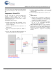
Device Initialization
This is the first user defined function in the initialization
sequence. The function main() is the C programming
language entry for the FX3 firmware. Three main actions
are performed in this function.
1. Device initialization: This is the first step in the
main().
status = CyU3PDeviceInit (NULL);
if (status != CY_U3P_SUCCESS)
{
goto handle_fatal_error;
}
As part of the device initialization:
a. The CPU clock is setup. A NULL is passed as an
argument for CyU3PDeviceInit() that selects
the default clock configuration.
b. The VIC is initialized
c. The GCTL and the PLLs are configured.
The device initialization functions is part of the FX3
library
2. Device cache configuration: The second step is to
configure the device caches. The device has 8 KB
data cache and 8 KB instruction cache. In this
example, only instruction cache is enabled as the data
cache that is useful only when there is a large amount
of CPU based memory accesses. When used in
simple cases, the CPU can decrease performance
due to large number of cache flushes, and then cleans
and it also adds complexity to the code.
status = CyU3PDeviceCacheControl
(CyTrue, CyFalse, CyFalse);
{
goto handle_fatal_error;
}
3. I/O matrix configuration: The third step is the
configuration of the I/Os that are required. This
includes the GPIF and the serial interfaces (SPI, I
2
C,
I
2
S, GPIO, and UART).
io_cfg.isDQ32Bit = CyFalse;
io_cfg.useUart = CyTrue;
io_cfg.useI2C = CyFalse;
io_cfg.useI2S = CyFalse;
io_cfg.useSpi = CyFalse;
io_cfg.lppMode =
CY_U3P_IO_MATRIX_LPP_UART_ONLY;
/* No GPIOs are enabled. */
io_cfg.gpioSimpleEn[0] = 0;
io_cfg.gpioSimpleEn[1] = 0;
io_cfg.gpioComplexEn[0] = 0;
io_cfg.gpioComplexEn[1] = 0;
status = CyU3PDeviceConfigureIOMatrix
(&io_cfg);
if (status != CY_U3P_SUCCESS)
{
goto handle_fatal_error;
}
In this bulkloop example:
a. 16 bit data bus
b. GPIO, I
2
C, I
2
S, and SPI are not used
c. UART is used
The I/O matrix configuration data structure is
initialized and the