
Datasheet


Migrating from EZ-USB
®
FX2LP™ Based Design to EZ-USB FX3 Based Design
www.cypress.com Document No. 001-76348 Rev. ** 3
Differences in Hardware Level
Booting Options
EZ-USB FX2LP can boot from USB and I
2
C only. But
EZ-USB FX3 can load boot images from various sources,
selected by the configuration of the PMODE pins. The
boot options for EZ-USB FX3 are listed as follows:
Boot from USB
Boot from I
2
C
Boot from SPI (SPI devices supported are M25P16
(16 Mbit), M25P80 (8 Mbit), and M25P40 (4 Mbit) or
their equivalents
Boot from GPIF II Async ADMUX mode
Boot from GPIF II Sync ADMUX mode
Boot from GPIF II Async SRAM mode
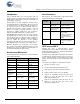
PMODE[2:0] Boot From
F00 Sync ADMUX (16-bit)
F01 Async ADMUX (16-bit)
F11 USB boot
F0F Async SRAM (16-bit)
F1F I
2
C, On Failure, USB boot is
enabled
1FF I
2
C only
0F1 SPI, on Failure, USB boot is
enabled.
If an external EEPROM is used on the I
2
C bus for firmware
image booting, 1 kΩ pull-up resistors should be placed on
the SCL and SDA lines for up to 1 MHz EEPROM
communication.
We recommend adding pull-up and pull-down options on
the PMODE [2:0] signals and load the combination
needed for preferred booting option. Adding the options
gives the flexibility to debug the system during early
development.
Crystal / Clock
EZ-USB FX2LP supports only crystal input, where as
EZ-USB FX3 supports external clock input along with the
crystal support. The following table lists the details of the
clock or crystal inputs that these two devices accept.
EZ-USB FX2LP EZ-USB FX3
External
clock
Not supported 19.2, 26, 38.4, and
52 MHz
Crystal
24MHz 19.2 MHz
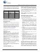
Based on the clocking option that is used, the FSLC[2:0]
lines can be tied to power, through a weak pull-up resistor,
or to ground. The following table shows the values of
FSLC[2:0] for the different clocking options.
FSLC[2] FSLC[1] FSLC[0] Crystal/Clock
0 0 0 19.2 MHz crystal
1 0 0 19.2 MHz input clock
1 0 1 26 MHz input clock
1 1 0 38.4 MHz input clock
1 1 1 52 MHz input clock
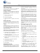
Power Supply Configurations and
Decoupling Capacitance
The table below shows the different power domains and
the voltage settings on each of these domains for FX3.
Parameter Description
Min
(V)
Max
(V)
Notes
V
DD
Core voltage
supply
1.15 1.25 1.2 V
typical
A
VDD
Analog voltage
supply
1.15 1.25 1.2 V
typical
V
IO1
GPIF II I/O power
domain
1.7 3.6 1.8, 2.5
and 3.3 V
typical
V
IO2
IO2 power domain 1.7 3.6 1.8, 2.5
and 3.3 V
typical
V
IO3
IO3 power domain 1.7 3.6 1.8, 2.5
and 3.3 V
typical
V
IO4
UART/SPI/I
2
S
power domain
1.7 3.6 1.8, 2.5
and 3.3 V
typical
V
IO5
I
2
C and JTAG
supply domain
1.15 3.6 1.2, 1.8,
2.5 and 3.3
V typical
V
BATT
USB voltage
supply
3.2 6 3.7 V
typical
V
BUS
USB voltage
supply
4.1 6 5 V typical
C
VDDQ
Clock voltage
supply
1.7 3.6 1.8, 3.3 V
typical
U3TX
VDDQ
USB3.0 1.2 V
supply
1.15 1.25 1.2 V
typical
U3RX
VDDQ
USB3.0 1.2 V
supply
1.15 1.25 1.2 V
typical