
Specifications

CY7C6431x
CY7C6434x
CY7C6435x
Document Number: 001-12394 Rev. *R Page 5 of 40
SPI configuration register (SPI_CFG) sets master/slave
functionality, clock speed, and interrupt select. SPI control
register (SPI_CR) provides four control bits and four status bits
for device interfacing and synchronization.
The SPIM hardware has no support for driving the Slave Select
(SS_) signal. The behavior and use of this signal is dependent
on the application and enCoRe V device and, if required, must
be implemented in firmware.
There is an additional data input in the SPIS, Slave Select (SS_),
which is an active low signal. SS_ must be asserted to enable
the SPIS to receive and transmit. SS_ has two high level
functions:
■ To allow for the selection of a given slave in a multi-slave
environment.
■ To provide additional clocking for TX data queuing in SPI modes
0 and 1.
I
2
C Slave
The I
2
C slave enhanced communications block is a
serial-to-parallel processor, designed to interface the enCoRe V
device to a two-wire I
2
C serial communications bus. To eliminate
the need for excessive CPU intervention and overhead, the block
provides I
2
C-specific support for status detection and generation
of framing bits. By default, the I
2
C slave enhanced module is
firmware compatible with the previous generation of I
2
C slave
functionality. However, this module provides new features that
are configurable to implement significant flexibility for both
internal and external interfacing. The basic I
2
C features include:
■ Slave, transmitter, and receiver operation.
■ Byte processing for low CPU overhead.
■ Interrupt or polling CPU interface.
■ Support for clock rates of up to 400 kHz.
■ 7- or 10-bit addressing (through firmware support).
■ SMBus operation (through firmware support).
Enhanced features of the I
2
C Slave Enhanced Module include:
■ Support for 7-bit hardware address compare.
■ Flexible data buffering schemes.
■ A “no bus stalling” operating mode.
■ A low power bus monitoring mode.
The I
2
C block controls the data (SDA) and the clock (SCL) to the
external I
2
C interface through direct connections to two
dedicated GPIO pins. When I
2
C is enabled, these GPIO pins are
not available for general purpose use. The enCoRe V CPU
firmware interacts with the block through I/O register reads and
writes, and firmware synchronization is implemented through
polling and/or interrupts.
In the default operating mode, which is firmware compatible with
previous versions of I
2
C slave modules, the I
2
C bus is stalled
upon every received address or byte, and the CPU is required to
read the data or supply data as required before the I
2
C bus
continues. However, this I
2
C Slave Enhanced module provides
new data buffering capability as an enhanced feature. In the
EZI
2
C buffering mode, the I
2
C slave interface appears as a
32-byte RAM buffer to the external I
2
C master. Using a simple
predefined protocol, the master controls the read and write
pointers into the RAM. When this method is enabled, the slave
never stalls the bus. In this protocol, the data available in the
RAM (this is managed by the CPU) is valid.
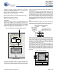
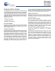
Figure 5. I
2
C Block Diagram
I2C Core
I2C Basic
Configuration
I2C_CFG
I2C_SCR
I2C_DR
Plus Features
HW Addr Cmp
Buffer Module
CPU Port
Buffer Ctl
32 Byte RAM
I2C Plus
Slave
I2C_ADDR
SDA_OUT
SCL_IN
SYSCLK
I2C_EN
To/From
GPIO
Pins
STANDBY
SCL_OUT
SDA_IN
I2C_XSTAT
I2C_XCFG
I2C_BUF
I2C_BP
I2C_CP
MCU_CP
MCU_BP
System Bus