
Specifications

CY7C6431x
CY7C6434x
CY7C6435x
Document Number: 001-12394 Rev. *R Page 4 of 40
Firmware is required to handle various parts of the USB
interface. The SIE issues interrupts after key USB events to
direct firmware to appropriate tasks:
■ Fill and empty the USB data buffers in USB SRAM.
■ Enable PMA channels appropriately.
■ Coordinate enumeration by decoding USB device requests.
■ Suspend and resume coordination.
■ Verify and select data toggle values.
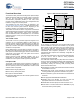
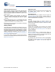
10-bit ADC
The ADC on enCoRe V device is an independent block with a
state machine interface to control accesses to the block. The
ADC is housed together with the temperature sensor core and
can be connected to this or the Analog mux bus. As a default
operation, the ADC is connected to the temperature sensor
diodes to give digital values of the temperature.
Figure 2. ADC System Performance Block Diagram
The ADC User Module contains an integrator block and one
comparator with positive and negative input set by the MUXes.
The input to the integrator stage comes from the analog global
input mux or the temperature sensor with an input voltage range
of 0 V to V
REFADC
.
In the ADC only configuration (the ADC MUX selects the Analog
mux bus, not the default temperature sensor connection), an
external voltage can be connected to the input of the modulator
for voltage conversion. The ADC is run for a number of cycles
set by the timer, depending upon the desired resolution of the
ADC. A counter counts the number of trips by the comparator,
which is proportional to the input voltage. The Temp Sensor block
clock speed is 36 MHz and is divided down to 1 to 12 MHz for
ADC operation.
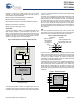
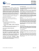
SPI
The serial peripheral interconnect (SPI) 3-wire protocol uses
both edges of the clock to enable synchronous communication
without the need for stringent setup and hold requirements.
Figure 3. Basic SPI Configuration
A device can be a master or slave. A master outputs clock and
data to the slave device and inputs slave data. A slave device
inputs clock and data from the master device and outputs data
for input to the master. Together, the master and slave are
essentially a circular Shift register, where the master generates
the clocking and initiates data transfers.
A basic data transfer occurs when the master sends eight bits of
data, along with eight clocks. In any transfer, both master and
slave transmit and receive simultaneously. If the master only
sends data, the received data from the slave is ignored. If the
master wishes to receive data from the slave, the master must
send dummy bytes to generate the clocking for the slave to send
data back.
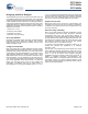
Figure 4. SPI Block Diagram
INTERFACE BLOCK
COMMAND/ STATUS
ADC
TEMP
DIODES
V
IN
SYSTEM BUS
TEMP SENSOR/ ADC
Interface to the M8 C
( Processor ) Core
SPI Master SPI Slave
MOSI
MISO
SCLK
Data is output by
both the Master
and Slave on
one edge of the
clock.
Data is registered at the
input of both devices on the
opposite edge of the clock.
SPI Block
Registers
SYSCLK
DATA_OUTDATA_IN
CLK_IN CLK_OUT
INT
SS_
SCLK
MOSI,
MISO
SCLK
MOSI,
MISO
CONFIGURATION[7:0] CONTROL[7:0]
TRANSMIT[7:0] RECEIVE[7:0]