
Specifications

CY7C6431x
CY7C6434x
CY7C6435x
Document Number: 001-12394 Rev. *R Page 31 of 40
Package Handling
Some IC packages require baking before they are soldered onto a PCB to remove moisture that may have been absorbed after leaving
the factory. A label on the package has details about the actual bake temperature and the minimum bake time to remove this moisture.
The maximum bake time is the aggregate time that the parts exposed to the bake temperature. Exceeding this exposure may degrade
device reliability.
Thermal Impedances
Capacitance on Crystal Pins
Solder Reflow Peak Temperature
Following is the minimum solder reflow peak temperature to achieve good solderability.
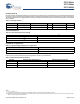
Table 24. Package Handling
Parameter Description Minimum Typical Maximum Unit
TBAKETEMP Bake temperature – 125 See package label
C
TBAKETIME Bake time See package label – 72 hours
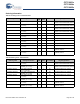
Table 25. Thermal Impedances per Package
Package Typical
JA
[21]
16-pin QFN 32.69 C / W
32-pin QFN
[22]
19.51 C / W
48-pin QFN
[22]
17.68 C / W
Table 26. Typical Package Capacitance on Crystal Pins
Package Package Capacitance
32-pin QFN 3.2 pF
48-pin QFN 3.3 pF
Table 27. Solder Reflow Peak Temperature
Package Minimum Peak Temperature
[23]
Maximum Peak Temperature
16-pin QFN 240 C 260 C
32-pin QFN 240 C 260 C
48-pin QFN 240 C 260 C
Notes
21. T
J
= T
A
+ Power x
JA.
22. To achieve the thermal impedance specified for the package, solder the center thermal pad to the PCB ground plane.
23. Higher temperatures may be required based on the solder melting point. Typical temperatures for solder are 220 ± 5 °C with Sn-Pb or 245 ± 5 °C with Sn-Ag-Cu paste.
Refer to the solder manufacturer specifications.