
Specifications

CY7C6431x
CY7C6434x
CY7C6435x
Document Number: 001-12394 Rev. *R Page 3 of 40
Functional Overview
The enCoRe V family of devices are designed to replace multiple
traditional full-speed USB microcontroller system components
with one, low cost single-chip programmable component.
Communication peripherals (I
2
C/SPI), a fast CPU, Flash
program memory, SRAM data memory, and configurable I/O are
included in a range of convenient pinouts.
The architecture for this device family, as illustrated in the
enCoRe V Block Diagram on page 1, consists of two main areas:
the CPU core and the system resources. Depending on the
enCoRe V package, up to 36 GPIO are also included.
This product is an enhanced version of Cypress’s successful full
speed-USB peripheral controllers. Enhancements include faster
CPU at lower voltage operation, lower current consumption,
twice the RAM and Flash, hot-swappable I/Os, I
2
C hardware
address recognition, new very low current sleep mode, and new
package options.
The enCoRe V Core
The enCoRe V Core is a powerful engine that supports a rich
instruction set. It encompasses SRAM for data storage, an
interrupt controller, sleep and watchdog timers, and IMO and
ILO. The CPU core, called the M8C, is a powerful processor with
speeds up to 24 MHz. The M8C is a four-MIPS, 8-bit Harvard
architecture microprocessor.
During USB operation, the CPU speed can be set to any setting.
Be aware that USB throughput decreases with a decrease in
CPU speed. For maximum throughput, the CPU clock should be
made equal to the system clock. The system clock must be
24 MHz for USB operation.
System resources provide additional capability, such as a
configurable I
2
C slave and SPI master-slave communication
interface and various system resets supported by the M8C.
Full-Speed USB
The enCoRe V USB system resource adheres to the USB 2.0
Specification for full speed devices operating at 12 Mb/second
with one upstream port and one USB address. enCoRe V USB
consists of these components:
■ Serial interface engine (SIE) block.
■ PSoC memory arbiter (PMA) block.
■ 512 bytes of dedicated SRAM.
■ A full-speed USB Transceiver with internal regulator and two
dedicated USB pins.
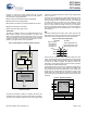
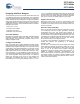
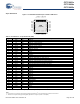
Figure 1. USB Transceiver Regulator
At the enCoRe V system level, the full-speed USB system
resource interfaces to the rest of the enCoRe V by way of the
M8C’s register access instructions and to the outside world by
way of the two USB pins. The SIE supports nine endpoints
including a bidirectional control endpoint (endpoint 0) and eight
unidirectional data endpoints (endpoints 1 to 8). The
unidirectional data endpoints are individually configurable as
either IN or OUT.
Low value series resistors R
EXT
(22 Ω) must be added externally
to the D+ and D– lines to meet the driving impedance
requirement for full-speed USB.
The USB Serial Interface Engine (SIE) allows the enCoRe V
device to communicate with the USB host at full speed data rates
(12 Mb/s). The SIE simplifies the interface to USB traffic by
automatically handling the following USB processing tasks
without firmware intervention:
■ Translates the encoded received data and formats the data to
be transmitted on the bus.
■ Generates and checks cyclical redundancy checks (CRCs).
Incoming packets failing checksum verification are ignored.
■ Checks addresses. Ignores all transactions not addressed to
the device.
■ Sends appropriate ACK/NAK/Stall handshakes.
■ Identifies token type (SETUP, IN, OUT) and sets the
appropriate token bit once a valid token in received.
■ Identifies Start-of-Frame (SOF) and saves the frame count.
■ Sends data to or retrieves data from the USB SRAM, by way
of the PSoC Memory Arbiter (PMA).
VOLTAGE
REGULATOR
5V 3.3V
1.5K 5K
PS2 Pull Up
DP
DM
TEN
TD
PDN
RD
DPO
RSE0
DMO
RECEIVERS
TRANSMITTER