
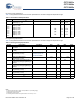
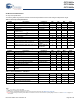
Specifications
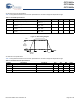
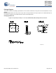

CY7C6431x
CY7C6434x
CY7C6435x
Document Number: 001-12394 Rev. *R Page 24 of 40
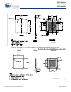
AC Programming Specifications
Tab l e 2 0 lists guaranteed maximum and minimum specifications for the entire voltage and temperature ranges.
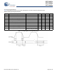
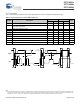
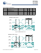
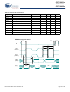
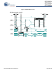
Figure 12. Timing Diagram - AC Programming Cycle
Table 20. AC Programming Specifications
Symbol Description Conditions Min Typ Max Units
T
RSCLK
Rise time of SCLK 1 – 20 ns
T
FSCLK
Fall time of SCLK 1 – 20 ns
T
SSCLK
Data setup time to falling edge of SCLK 40 – – ns
T
HSCLK
Data hold time from falling edge of SCLK 40 – – ns
F
SCLK
Frequency of SCLK 0 – 8 MHz
T
ERASEB
Flash erase time (Block) – – 18 ms
T
WRITE
Flash block write time – – 25 ms
T
DSCLK1
Data out delay from falling edge of SCLK, V
DD
> 3.6 V – – 60 ns
T
DSCLK2
Data out delay from falling edge of SCLK 3.0 V < V
DD
< 3.6 V – – 85 ns
T
XRST3
External reset pulse width after power-up Required to enter programming
mode when coming out of sleep
263 – – s