
Specifications

CY7C6431x
CY7C6434x
CY7C6435x
Document Number: 001-12394 Rev. *R Page 22 of 40
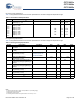
AC Electrical Characteristics
AC Chip Level Specifications
The following tables list guaranteed maximum and minimum specifications for the entire voltage and temperature ranges.
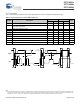
Table 15. AC Chip Level Specifications
Symbol Description Conditions Min Typ Max Units
F
CPU
Processing frequency
[16]
5.7 – 25.2 MHz
F
32K1
Internal low-speed oscillator (ILO) frequency Trimmed
[17]
19 32 50 kHz
F
32K_U
ILO untrimmed frequency) 13 32 82 kHz
F
32K2
ILO frequency Untrimmed 13 32 82 kHz
F
IMO24
Internal main oscillator (IMO) stability for
24 MHz ± 5%
(12)
22.8 24 25.2 MHz
F
IMO12
IMO stability for 12 MHz
[17]
11.4 12 12.6 MHz
F
IMO6
IMO stability for 6 MHz
[17]
5.7 6.0 6.3 MHz
DC
IMO
Duty cycle of IMO 40 50 60 %
DC
ILO
ILO duty cycle 40 50 60 %
SR
POWER_UP
Power supply slew rate – – 250 V/ms
T
XRST
External reset pulse width at power-up After supply voltage
is valid
1 – – ms
T
XRST2
External reset pulse width after power-up
[18]
Applies after part
has booted
10 – – s
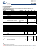
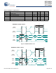
Table 16. AC Characteristics – USB Data Timings
Symbol Description Conditions Min Typ Max Units
Tdrate Full speed data rate Average bit rate 11.97 12 12.03 MHz
Tdjr1 Receiver data jitter tolerance To next transition –18.5 – 18.5 ns
Tdjr2 Receiver data jitter tolerance To pair transition –9 – 9 ns
Tudj1 Driver differential jitter To next transition –3.5 – 3.5 ns
Tudj2 Driver differential jitter To pair transition –4.0 – 4.0 ns
Tfdeop Source jitter for differential transition To SE0 transition –2 – 5 ns
Tfeopt Source SE0 interval of EOP 160 – 175 ns
Tfeopr Receiver SE0 interval of EOP 82 – – ns
Tfst Width of SE0 interval during differential
transition
––14ns
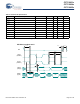
Table 17. AC Characteristics – USB Driver
Symbol Description Conditions Min Typ Max Units
Tr Transition rise time 50 pF 4 – 20 ns
Tf Transition fall time 50 pF 4 – 20 ns
TR
[19]
Rise/fall time matching 90.00 – 111.1 %
Vcrs Output signal crossover voltage 1.3 – 2.0 V
Notes
16. V
DD
= 3.0 V and T
J
= 85 C, CPU speed.
17. Trimmed for 3.3 V operation using factory trim values.
18. The minimum required XRES pulse length is longer when programming the device (see
Table 20 on page 24).
19. Errata: Rising to falling rate matching of the USB D+ and D- lines has a corner case issue when operating voltage is below 3.3 V. Refer to “Errata” on page 35 for
more details.