
Specifications

CY7C6431x
CY7C6434x
CY7C6435x
Document Number: 001-12394 Rev. *R Page 21 of 40
DC POR and LVD Specifications
Tab l e 1 3 lists guaranteed maximum and minimum specifications for the entire voltage and temperature ranges.
DC Programming Specifications
Tab l e 1 4 lists guaranteed maximum and minimum specifications for the entire voltage and temperature ranges.
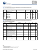
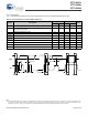
Table 13. DC POR and LVD Specifications
Symbol Description Conditions Min Typ Max Units
V
PPOR
V
DD
value for PPOR trip
[12]
PORLEV[1:0] = 10b – 2.82 2.95 V
V
LVD0
V
LVD1
V
LVD2
V
LVD3
V
LVD4
V
LVD5
V
LVD6
V
LVD7
V
DD
value for LVD trip
VM[2:0] = 000b
VM[2:0] = 001b
VM[2:0] = 010b
VM[2:0] = 011b
VM[2:0] = 100b
VM[2:0] = 101b
VM[2:0] = 110b
VM[2:0] = 111b
–
–
2.85
2.95
3.06
–-
–
4.62
–
–
2.92
3.02
3.13
–
–
4.73
–
–
2.99
3.09
3.20
–
–
4.83
V
V
V
V
V
V
V
V
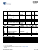
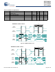
Table 14. DC Programming Specifications
Symbol Description Conditions Min Typ Max Units
V
DDIWRITE
Supply voltage for flash write
operations
1.71 – 5.25 V
I
DDP
Supply current during programming
or verify
– 5 25 mA
V
ILP
Input low voltage during
programming or verify
See appropriate DC
General Purpose I/O
Specifications table
– – V
IL
V
V
IHP
Input high voltage during
programming or verify
1.71 – V
DDIWRITE
+ 0.3 V
I
ILP
Input current when applying Vilp to
P1[0] or P1[1] during programming or
verify
[13]
– – 0.2 mA
I
IHP
Input current when applying Vihp to
P1[0] or P1[1] during programming or
verify
[13]
– – 1.5 mA
V
OLP
Output low voltage during
programming or verify
– – V
SS
+ 0.75 V
V
OHP
Output high voltage during
programming or verify
V
DDIWRITE
– 0.9 – V
DDIWRITE
V
Flash
ENPB
Flash write endurance
[14]
50,000 – – Cycles
Flash
DR
Flash data retention
[15]
10 20 – Years
Notes
12. Always greater than 50 mV above V
PPOR
(PORLEV = 10) for falling supply.
13. Driving internal pull down resistor.
14. Erase/write cycles per block.
15. Following maximum Flash write cycles at Tamb = 55 °C and Tj = 70 °C.