
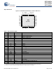
Specifications

CY7C6431x
CY7C6434x
CY7C6435x
Document Number: 001-12394 Rev. *R Page 20 of 40
DC General Purpose I/O Specifications
Tab l e 1 2 lists guaranteed maximum and minimum specifications for the voltage and temperature ranges: 3.0 V to 5.5 V and package
specific temperature range. Typical parameters apply to 5 V and 3.3 V at 25 °C. These are for design guidance only.
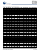
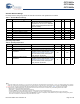
Table 12. 3.0 V and 5.5 V DC GPIO Specifications
Symbol Description Conditions Min Typ Max Units
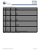
R
PU
Pull-up resistor 4 5.6 8 k
V
OH1
High output voltage
Port 2 or 3 pins
I
OH
< 10 µA, maximum of 10 mA source
current in all I/Os.
V
DD
– 0.2 – – V
V
OH2
High output voltage
Port 2 or 3 Pins
I
OH
= 1 mA, maximum of 20 mA source
current in all I/Os.
V
DD
– 0.9 – – V
V
OH3
High output voltage
Port 0 or 1 pins with LDO regulator
disabled
I
OH
< 10 µA, maximum of 10 mA source
current in all I/Os.
V
DD
– 0.2 – – V
V
OH4
High output voltage
Port 0 or 1 pins with LDO regulator
disabled
I
OH
= 5 mA, maximum of 20 mA source
current in all I/Os.
V
DD
– 0.9 – – V
V
OH5
High output voltage
Port 1 pins with LDO regulator enabled
for 3 V Out
I
OH
< 10 A, V
DD
> 3.1 V, maximum of
4 I/Os all sourcing 5 mA
2.85 3.00 3.3 V
V
OH6
High output voltage
Port 1 pins with LDO regulator enabled
for 3 V out
I
OH
= 5 mA, V
DD
> 3.1 V, maximum of
20 mA source current in all I/Os
2.20 – – V
V
OH7
High output voltage
Port 1 pins with LDO enabled for 2.5 V
out
I
OH
< 10 A, V
DD
> 3.0 V, maximum of
20 mA source current in all I/Os
2.35 2.50 2.75 V
V
OH8
High output voltage
Port 1 pins with LDO enabled for 2.5 V
out
I
OH
= 2 mA, V
DD
> 3.0 V, maximum of
20 mA source current in all I/Os
1.90 – – V
V
OH9
High output voltage
Port 1 pins with LDO enabled for 1.8 V
out
I
OH
< 10 A, V
DD
> 3.0 V, maximum of
20 mA source current in all I/Os
1.60 1.80 2.1 V
V
OH10
High output voltage
Port 1 pins with LDO enabled for 1.8 V
out
I
OH
= 1 mA, V
DD
> 3.0 V, maximum of
20 mA source current in all I/Os
1.20 – – V
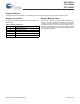
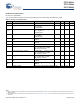
V
OL
Low output voltage I
OL
= 25 mA, V
DD
> 3.3 V, maximum of
60 mA sink current on even port pins
(for example, P0[2] and P1[4]) and 60
mA sink current on odd port pins (for
example, P0[3] and P1[5]).
– – 0.75 V
V
IL
Input low voltage – – 0.8 V
V
IH
Input high voltage 2.0 – – V
V
H
Input hysteresis voltage –80–mV
I
IL
Input leakage (absolute value) – 0.001 1 µA
C
PIN
Pin capacitance Package and pin dependent.
Te mp = 2 5
C.
0.5
1.7 5 pF