
Specifications

CY7C6431x
CY7C6434x
CY7C6435x
Document Number: 001-12394 Rev. *R Page 17 of 40
Absolute Maximum Ratings
Exceeding maximum ratings may shorten the useful life of the device. User guidelines are not tested.
Operating Temperature
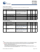
Table 7. Absolute Maximum Ratings
Symbol Description Conditions Min Typ Max Units
T
STG
Storage temperature
[10]
Higher storage temperatures reduces data
retention time. Recommended Storage
Temperature is +25 °C ± 25 °C. Extended
duration storage temperatures above 85
C
degrades reliability.
–55 +25 +125 °C
V
DD
Supply voltage relative to V
SS
–0.5 – +6.0 V
V
IO
DC input voltage V
SS
– 0.5 – V
DD
+ 0.5 V
V
IOZ
DC voltage applied to tristate V
SS
– 0.5 – V
DD
+ 0.5 V
I
MIO
Maximum current into any port pin –25 – +50 mA
ESD Electrostatic discharge voltage Human body model ESD 2000 – – V
LU
[8]
Latch up current In accordance with JESD78 standard – – 200 mA
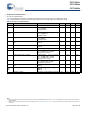
Table 8. Operating Temperature
Symbol Description Conditions Min Typ Max Units
T
AI
Ambient industrial temperature –40 – +85 °C
T
AC
Ambient commercial temperature 0 – +70 °C
T
JI
Operational industrial die
temperature
[11]
The temperature rise from ambient to junction
is package specific. Refer the table Thermal
Impedances per Package on page 31. The
user must limit the power consumption to
comply with this requirement.
–40 – +100 °C
T
JC
Operational commercial die
temperature
The temperature rise from ambient to junction
is package specific. Refer the table Thermal
Impedances per Package on page 31. The
user must limit the power consumption to
comply with this requirement.
0 – +85 °C
Notes
7. When V
DD
remains in the range from 1.71 V to 1.9 V for more than 50 µsec, the slew rate when moving from the 1.71 V to 1.9 V range to greater than 2 V must be
slower than 1 V/500 µsec to avoid triggering POR. The only other restriction on slew rates for any other voltage range or transition is the SRPOWER_UP parameter.
8. Errata: For Port 1 pins P1[1], P1[4], and P1[5] 300 Ohm external resistor is needed to meet this spec. Refer to “Errata” on page 35 for more details.
9. If powering down in standby sleep mode, to properly detect and recover from a V
DD
brown out condition any of the following actions must be taken:
• Bring the device out of sleep before powering down.
• Assure that V
DD
falls below 100 mV before powering back up.
• Set the No Buzz bit in the OSC_CR0 register to keep the voltage monitoring circuit powered during sleep.
• Increase the buzz rate to assure that the falling edge of V
DD
is captured. The rate is configured through the PSSDC bits in the SLP_CFG register.
For the referenced registers, refer to the enCoRe V Technical Reference Manual. In deep sleep mode, additional low power voltage monitoring circuitry allows
V
DD
brown out conditions to be detected for edge rates slower than 1 V/ms.