
Specifications

CY7C6431x
CY7C6434x
CY7C6435x
Document Number: 001-12394 Rev. *R Page 10 of 40
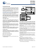
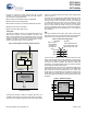
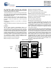
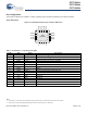
32-pin Part Pinout
Figure 7. CY7C64343/CY7C64345 32-pin enCoRe V USB Device
P0[1]
P2[5]
P2[3]
P2[1]
P1[7]
QFN
( Top View)
9
10
11
12
13
14
15
16
1
2
3
4
5
6
7
8
24
23
22
21
20
19
18
17
32
31
30
29
28
27
26
25
V
SS
P0[3]
P0[7]
V
DD
P0[6]
P0[4]
P0[2]
P1[5]
P1[1]
P0[0]
P2[6]
P3[0]
XRES
D+
D–
P1[0]
P1[2]
P1[4]
P1[6]
P2[4]
P2[2]
P2[0]
P3[2]
P0[5]
P1[3]
V
DD
V
SS
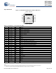
Table 2. Pin Definitions – 32-pin Part Pinout (QFN)
Pin No. Type Name Description
1 I/OH P0[1] Digital I/O
2 I/O P2[5] Digital I/O, crystal output (Xout)
3 I/O P2[3] Digital I/O, crystal Input (Xin)
4 I/O P2[1] Digital I/O
5 I/OHR P1[7] Digital I/O, I
2
C SCL, SPI SS
6 I/OHR P1[5] Digital I/O, I
2
C SDA, SPI MISO
7 I/OHR P1[3] Digital I/O, SPI CLK
8 I/OHR P1[1]
[3, 4]
Digital I/O, ISSP CLK, I
2
C SCL, SPI MOSI
9 Power V
SS
Ground
10 I/O D+ USB PHY
11 I/O D– USB PHY
12 Power V
DD
Supply voltage
13 I/OHR P1[0]
[3, 4]
Digital I/O, ISSP DATA, I
2
C SDA, SPI CLK
14 I/OHR P1[2] Digital I/O
15 I/OHR P1[4] Digital I/O, optional external clock input (EXTCLK)
16 I/OHR P1[6] Digital I/O
17 Reset XRES Active high external reset with internal pull down
18 I/O P3[0] Digital I/O
19 I/O P3[2] Digital I/O
20 I/O P2[0] Digital I/O
21 I/O P2[2] Digital I/O
22 I/O P2[4] Digital I/O
23 I/O P2[6] Digital I/O
24 I/OH P0[0] Digital I/O
25 I/OH P0[2] Digital I/O
26 I/OH P0[4] Digital I/O
27 I/OH P0[6] Digital I/O
28 Power V
DD
Supply voltage
29 I/OH P0[7] Digital I/O
30 I/OH P0[5] Digital I/O
31 I/OH P0[3] Digital I/O
32 Power V
SS
Ground
CP Power V
SS
Ensure the center pad is connected to ground
LEGEND I = Input, O = Output, OH = 5 mA High Output Drive, R = Regulated Output
Notes
3. During power up or reset event, device P1[0] and P1[1] may disturb the I
2
C bus. Use alternate pins if issues are encountered.
4. These are the in-system serial programming (ISSP) pins that are not High Z at power on reset (POR).