
Specifications

CY7C6431x
CY7C6434x
CY7C6435x
enCoRe™ V Full Speed USB Controller
Cypress Semiconductor Corporation • 198 Champion Court • San Jose, CA 95134-1709 • 408-943-2600
Document Number: 001-12394 Rev. *R Revised November 20, 2013
enCoRe™ V Full Speed USB Controller
Features
■ Powerful Harvard-architecture processor
❐ M8C processor speeds running up to 24 MHz
❐ Low power at high processing speeds
❐ Interrupt controller
❐ 3.0 V to 5.5 V operating voltage without USB
❐ Operating voltage with USB enabled:
• 3.15 V to 3.45 V when supply voltage is around 3.3 V
• 4.35 V to 5.25 V when supply voltage is around 5.0 V
❐ Commercial temperature range: 0°C to +70°C
❐ Industrial temperature range: –40 °C to +85 °C
■ Flexible on-chip memory
❐ Up to 32 KB flash program storage:
• 50,000 erase and write cycles
• Flexible protection modes
❐ Up to 2048 bytes SRAM data storage
❐ In-system serial programming (ISSP)
■ Complete development tools
❐ Free development tool PSoC Designer™
❐ Full-featured, in-circuit emulator and programmer
❐ Full-speed emulation
❐ Complex breakpoint structure
❐ 128-KB trace memory
■ Precision, programmable clocking
❐ Crystal-less oscillator with support for an external crystal or
resonator
❐ Internal ±5.0% 6, 12, or 24 MHz main oscillator (IMO):
• 0.25% accuracy with oscillator lock to USB data, no
external components required
• Internal low-speed oscillator (ILO) at 32 kHz for watchdog
and sleep. The frequency range is 19 to 50 kHz with a
32-kHz typical value
■ Programmable pin configurations
❐ Up to 36 general purpose I/O (GPIO) depending on package.
❐ 25 mA sink current on all GPIO
• 60mA total sink current on Even port pins and 60 mA total
sink current on Odd port pins
• 120 mA total sink current on all GPIOs
❐ Pull-up, High Z, open drain, CMOS drive modes on all GPIO
❐ CMOS drive mode A -5 mA source current on ports 0 and 1
and 1 mA on ports 2, 3, and 4
• 20 mA total source current on all GPIOs
❐ Low dropout voltage regulator for Port 1 pins:
• Programmable to output 3.0, 2.5, or 1.8 V
❐ Selectable, regulated digital I/O on Port 1
❐ Configurable input threshold for Port 1
❐ Hot-swappable Capability on Port 1
■ Full-Speed USB (12 Mbps)
❐ Eight unidirectional endpoints
❐ One bidirectional control endpoint
❐ USB 2.0-compliant: TID# 40000893
❐ Dedicated 512 bytes buffer
❐ No external crystal required
■ Additional system resources
❐ Configurable communication speeds
❐ I
2
C slave:
• Selectable to 50 kHz, 100 kHz, or 400 kHz
• Implementation requires no clock stretching
• Implementation during sleep modes with less than 100 A
• Hardware address detection
❐ SPI master and SPI slave:
• Configurable between 46.9 kHz and 12 MHz
❐ Three 16-bit timers
❐ 10-bit ADC used to monitor battery voltage or other signals
with external components
❐ Watchdog and sleep timers
❐ Integrated supervisory circuit
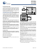
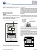
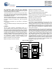
System Bus
6/12/24 MHz Internal Main Oscillator
CPU Core
(M8C)
SROM
8K/16K/32K Flash
SYSTEM RESOURCES
I2C Slave/SPI
Master-Slave
POR and LVD
System Resets
Port 1 Port 0
Sleep and
Watchdog
Full
Speed
USB
Port 3 Port 2
Prog. LDO
SRAM
2048 Bytes
Interrupt
Controller
enCoRe V
CORE
3 16-Bit
Timers
Port 4
ADC
enCoRe V Block Diagram
Errata: For information on silicon errata, see “Errata” on page 35. Details include trigger conditions, devices affected, and proposed workaround.