
User guide


CY7C601xx
CY7C602xx
Document 38-16016 Rev. *C Page 37 of 62
P1.0 Configuration
P1.1 Configuration
P1.2 Configuration
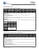
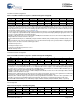
Table 54.P1.0 Configuration (P10CR) [0x0D] [R/W]
Bit # 7 6 5 4 3 2 1 0
Field Reserved Int Enable Int Act Low Reserved P1.0 and P1.1
Pull Up Enable
Output Enable
Read/Write R/W R/W R/W – ––– R/W
Default 0 0 0 0 000 0
This register controls the operation of the P1.0 pin.
Bit1: P1.0 and P1.1 Pull Up Enable
0 = Disable the P1.0 and P1.1 pull up resistors
1 = Enable the internal pull up resistors for both the P1.0 and P1.1. Each of the P1.0 and P1.1 pins is pulled up with R
UP1
(see
DC Characteristics on page 54)
Note: There is no 2-mA sourcing capability on this pin. The pin can only sink 5 mA at V
OL3
(see DC Characteristics on page 54)
The P1.0 is an open drain only output. It can actively drive a signal low, but cannot actively drive a signal high.
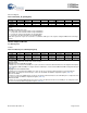
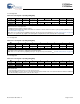
Table 55.P1.1 Configuration (P11CR) [0x0E] [R/W]
Bit # 7 6 5 4 3 2 1 0
Field Reserved Int Enable Int Act Low Reserved Open Drain Reserved Output Enable
Read/Write – R/W R/W – –R/W–R/W
Default 0 0 0 0 000 0
This register controls the operation of the P1.1 pin.
The pull up resistor on this pin is enabled by the P10CR Register
Note: There is no 2-mA sourcing capability on this pin. The pin can only sink 5 mA at V
OL3
(see DC Characteristics on page 54)
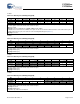
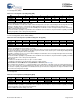
Table 56.P1.2 Configuration (P12CR) [0x0F] [R/W]
Bit # 7 6 5 4 3 2 1 0
Field CLK Output Int Enable Int Act Low TTL Threshold Reserved Open Drain Pull-up Enable Output Enable
Read/Write R/W R/W R/W R/W –R/WR/W R/W
Default 0 0 0 0 000 0
This register controls the operation of the P1.2
Bit 7: CLK Output
0 = The internally selected clock is not sent out onto P1.2 pin
1 = This CLK Output is used to observe connected external crystal oscillator clock connected in CY7C601xx. When CLK Output
is set, the internally selected clock is sent out onto P1.2 pin.