
User manual


CY8C29466, CY8C29566
CY8C29666, CY8C29866
Document Number: 38-12013 Rev. *M Page 37 of 47
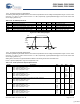
13. Packaging Information
This section illustrates the packaging specifications for the CY8C29x66 PSoC device, along with the thermal impedances for each
package and the typical package capacitance on crystal pins.
Important Note Emulation tools may require a larger area on the target PCB than the chip’s footprint. For a detailed description of
the emulation tools’ dimensions, refer to the document titled
PSoC Emulator Pod Dimensions at
http://www.cypress.com/design/MR10161.
13.1 Packaging Dimensions
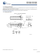
Figure 13-1. 28-Pin (300 mil) Molded DIP
DIMENSIONS IN INCHES[MM]
MIN.
MAX.
SEATING PLANE
0.260[6.60]
0.295[7.49]
0.090[2.28]
0.110[2.79]
0.055[1.39]
0.065[1.65]
0.015[0.38]
0.020[0.50]
0.015[0.38]
0.060[1.52]
0.120[3.05]
0.140[3.55]
0.009[0.23]
0.012[0.30]
0.310[7.87]
0.385[9.78]
0.290[7.36]
0.325[8.25]
0.030[0.76]
0.080[2.03]
0.115[2.92]
0.160[4.06]
0.140[3.55]
0.190[4.82]
1.345[34.16]
1.385[35.18]
3° MIN.
114
15 28
REFERENCE JEDEC MO-095
PART #
P28.3 STANDARD PKG.
LEAD FREE PKG.PZ28.3
LEAD END OPTION
SEE LEAD END OPTION
SEE LEAD END OPTION
(LEAD #1, 14, 15 & 28)
PACKAGE WEIGHT: 2.15gms
51-85014 *E
[+] Feedback