
User manual


CY8C29466, CY8C29566
CY8C29666, CY8C29866
Document Number: 38-12013 Rev. *M Page 13 of 47
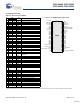
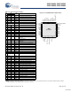
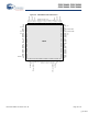
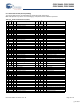
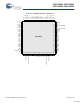
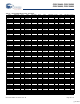
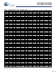
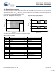
9.4 100-Pin Part Pinout
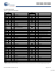
Table 9-5. 100-Pin Part Pinout (TQFP)
Pin
No.
Type
Name Description
Pin
No.
Type
Name Description
Digital Analog Digital Analog
1 NC No connection. 51 NC No connection.
2 NC No connection. 52 I/O P5[0]
3 I/O I P0[1] Analog column mux input. 53 I/O P5[2]
4 I/O P2[7] 54 I/O P5[4]
5 I/O P2[5] 55 I/O P5[6]
6 I/O I P2[3] Direct switched capacitor block input. 56 I/O P3[0]
7 I/O I P2[1] Direct switched capacitor block input. 57 I/O P3[2]
8 I/O P4[7] 58 I/O P3[4]
9 I/O P4[5] 59 I/O P3[6]
10 I/O P4[3] 60 NC No connection.
11 I/O P4[1] 61 NC No connection.
12 NC No connection. 62 Input XRES Active high external reset with internal pull
down.
13 NC No connection. 63 I/O P4[0]
14 Power SMP Switch Mode Pump (SMP) connection to
external components required.
64 I/O P4[2]
15 Power Vss Ground connection. 65 Power Vss Ground connection.
16 I/O P3[7] 66 I/O P4[4]
17 I/O P3[5] 67 I/O P4[6]
18 I/O P3[3] 68 I/O I P2[0] Direct switched capacitor block input.
19 I/O P3[1] 69 I/O I P2[2] Direct switched capacitor block input.
20 I/O P5[7] 70 I/O P2[4] External Analog Ground (AGND).
21 I/O P5[5] 71 NC No connection.
22 I/O P5[3] 72 I/O P2[6] External Voltage Reference (VREF).
23 I/O P5[1] 73 NC No connection.
24 I/O P1[7] I
2
C Serial Clock (SCL). 74 I/O I P0[0] Analog column mux input.
25 NC No connection. 75 NC No connection.
26 NC No connection. 76 NC No connection.
27 NC No connection. 77 I/O I/O P0[2] Analog column mux input and column output.
28 I/O P1[5] I
2
C Serial Data (SDA). 78 NC No connection.
29 I/O P1[3] 79 I/O I/O P0[4] Analog column mux input and column output.
30 I/O P1[1] Crystal (XTALin), I
2
C Serial Clock (SCL),
ISSP-SCLK*.
80 NC No connection.
31 NC No connection. 81 I/O I P0[6] Analog column mux input.
32 Power Vdd Supply voltage. 82 Power Vdd Supply voltage.
33 NC No connection. 83 Power Vdd Supply voltage.
34 Power Vss Ground connection. 84 Power Vss Ground connection.
35 NC No connection. 85 Power Vss Ground connection.
36 I/O P7[7] 86 I/O P6[0]
37 I/O P7[6] 87 I/O P6[1]
38 I/O P7[5] 88 I/O P6[2]
39 I/O P7[4] 89 I/O P6[3]
40 I/O P7[3] 90 I/O P6[4]
41 I/O P7[2] 91 I/O P6[5]
42 I/O P7[1] 92 I/O P6[6]
43 I/O P7[0] 93 I/O P6[7]
44 I/O P1[0] Crystal (XTALout), I
2
C Serial Data (SDA),
ISSP-SDATA*.
94 NC No connection.
45 I/O P1[2] 95 I/O I P0[7] Analog column mux input.
46 I/O P1[4] Optional External Clock Input (EXTCLK). 96 NC No connection.
47 I/O P1[6] 97 I/O I/O P0[5] Analog column mux input and column output.
48 NC No connection. 98 NC No connection.
49 NC No connection. 99 I/O I/O P0[3] Analog column mux input and column output.
50 NC No connection. 100 NC No connection.
LEGEND: A = Analog, I = Input, and O = Output.
* These are the ISSP pins, which are not High Z at POR (Power On Reset). See the PSoC Programmable System-on-Chip Technical Reference Manual for details.
[+] Feedback