
User manual

CY8C27143, CY8C27243
CY8C27443, CY8C27543, CY8C27643
Document Number: 38-12012 Rev. *O Page 39 of 53
AC Programming Specifications
The following table lists guaranteed maximum and minimum specifications for the voltage and temperature ranges: 4.75V to 5.25V
and -40°C ≤ T
A
≤ 85°C, or 3.0V to 3.6V and -40°C ≤ T
A
≤ 85°C, respectively. Typical parameters apply to 5V and 3.3V at 25°C and
are for design guidance only.
AC I
2
C Specifications
The following table lists guaranteed maximum and minimum specifications for the voltage and temperature ranges: 4.75V to 5.25V
and -40°C ≤ T
A
≤ 85°C, or 3.0V to 3.6V and -40°C ≤ T
A
≤ 85°C, respectively. Typical parameters apply to 5V and 3.3V at 25°C and
are for design guidance only.
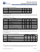
Table 40. 3.3V AC External Clock Specifications
Symbol Description Min Typ Max Unit
F
OSCEXT
Frequency with CPU Clock divide by 1
[19]
0.093 – 12.3 MHz
F
OSCEXT
Frequency with CPU Clock divide by 2 or greater
[20]
0.186 – 24.6 MHz
– High Period with CPU Clock divide by 1 41.7
– 5300 ns
– Low Period with CPU Clock divide by 1 41.7
– –ns
– Power Up IMO to Switch 150
– –
μ
s
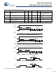
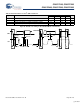
Table 41. AC Programming Specifications
Symbol Description Min Typ Max Unit Notes
T
RSCLK
Rise Time of SCLK 1 – 20 ns
T
FSCLK
Fall Time of SCLK 1 – 20 ns
T
SSCLK
Data Set up Time to Falling Edge of SCLK 40 – – ns
T
HSCLK
Data Hold Time from Falling Edge of SCLK 40 – – ns
F
SCLK
Frequency of SCLK 0 – 8 MHz
T
ERASEB
Flash Erase Time (Block) – 30 – ms
T
WRITE
Flash Block Write Time – 10 – ms
T
DSCLK
Data Out Delay from Falling Edge of SCLK – – 45 ns Vdd
>
3.6
T
DSCLK3
Data Out Delay from Falling Edge of SCLK – – 50 ns 3.0
≤
Vdd
≤
3.6
T
ERASEALL
Flash Erase Time (Bulk) – 95 – ms Erase all Blocks and
protection fields at once
T
PROGRAM_HOT
Flash Block Erase + Flash Block Write Time – – 80
[21]
ms 0°C <= Tj <= 100°C
T
PROGRAM_COLD
Flash Block Erase + Flash Block Write Time – – 160
[21]
ms -40°C <= Tj <= 0°C
Table 42. AC Characteristics of the I
2
C SDA and SCL Pins
Symbol Description
Standard Mode Fast Mode
Unit
Min Max Min Max
F
SCLI2C
SCL Clock Frequency 0 100 0 400 kHz
T
HDSTAI2C
Hold Time (repeated) START Condition. After this period, the first
clock pulse is generated.
4.0 –0.6– μs
T
LOWI2C
LOW Period of the SCL Clock 4.7 –1.3– μs
T
HIGHI2C
HIGH Period of the SCL Clock 4.0 –0.6– μs
T
SUSTAI2C
Set-up Time for a Repeated START Condition 4.7 –0.6– μs
T
HDDATI2C
Data Hold Time 0 –0– μs
Note
22. A Fast-Mode I2C-bus device can be used in a Standard-Mode I2C-bus system, but the requirement t
SU;DAT
≥ 250 ns must then be met. This is automatically the
case if the device does not stretch the LOW period of the SCL signal. If such device does stretch the LOW period of the SCL signal, it must output the next data bit
to the SDA line t
rmax
+ t
SU;DAT
= 1000 + 250 = 1250 ns (according to the Standard-Mode I2C-bus specification) before the SCL line is released.
[+] Feedback