
User manual

CY8C27143, CY8C27243
CY8C27443, CY8C27543, CY8C27643
Document Number: 38-12012 Rev. *O Page 37 of 53
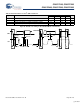
AC Analog Output Buffer Specifications
The following tables list guaranteed maximum and minimum specifications for the voltage and temperature ranges: 4.75V to 5.25V
and -40°C ≤ T
A
≤ 85°C, or 3.0V to 3.6V and -40°C ≤ T
A
≤ 85°C, respectively. Typical parameters apply to 5V and 3.3V at 25°C and
are for design guidance only.
Dead
Band
Kill Pulse Width:
Asynchronous Restart Mode 20 – – ns
Synchronous Restart Mode 50
[17]
– – ns
Disable Mode 50
[17]
– – ns
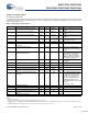
Maximum Frequency – – 49.2 MHz 4.75V < Vdd < 5.25V
CRCPRS
(PRS
Mode)
Maximum Input Clock Frequency – – 49.2 MHz 4.75V < Vdd < 5.25V
CRCPRS
(CRC
Mode)
Maximum Input Clock Frequency – – 24.6 MHz
SPIM Maximum Input Clock Frequency – – 8.2 MHz Maximum data rate at 4.1 MHz due
to 2 x over clocking.
SPIS Maximum Input Clock Frequency – – 4.1 MHz
Width of SS_ Negated Between Transmis-
sions
50
[17]
– – MHz
Trans-
mitter
Maximum Input Clock Frequency
[17]
Silicon A
Silicon B
Silicon B Maximum Input Clock Frequency with
Vdd ≥ 4.75V, 2 Stop Bits
–
–
–
–
–
–
16.4
24.6
49.2
MHz
MHz
MHz
Maximum data rate at 2.05 MHz
due to 8 x over clocking.
Maximum data rate at 3.08 MHz
due to 8 x over clocking.
Maximum data rate at 6.15 MHz
due to 8 x over clocking.
Receiver Maximum Input Clock Frequency
[18]
Silicon A
Silicon B
Silicon B Maximum Input Clock Frequency with
Vdd ≥ 4.75V, 2 Stop Bits
–
–
–
–
–
–
16.4
24.6
49.2
MHz
MHz
MHz
Maximum data rate at 2.05 MHz
due to 8 x over clocking.
Maximum data rate at 3.08 MHz
due to 8 x over clocking.
Maximum data rate at 6.15 MHz
due to 8 x over clocking.
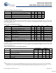
Table 36. AC Digital Block Specifications (continued)
Function Description Min Typ Max Unit Notes
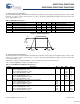
Table 37. 5V AC Analog Output Buffer Specifications
Symbol Description Min Typ Max Unit
T
ROB
Rising Settling Time to 0.1%, 1V Step, 100 pF Load
Power = Low
Power = High
–
–
–
–
2.5
2.5
μs
μs
T
SOB
Falling Settling Time to 0.1%, 1V Step, 100 pF Load
Power = Low
Power = High
–
–
–
–
2.2
2.2
μs
μs
[+] Feedback