
User manual

CY8C27143, CY8C27243
CY8C27443, CY8C27543, CY8C27643
Document Number: 38-12012 Rev. *O Page 35 of 53
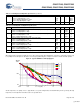
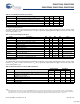
When bypassed by a capacitor on P2[4], the noise of the analog ground signal distributed to each block is reduced by a factor of up
to 5 (14 dB). This is at frequencies above the corner frequency defined by the on-chip 8.1k resistance and the external capacitor.
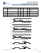
Figure 18. Typical AGND Noise with P2[4] Bypass
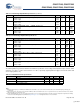
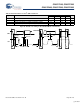
At low frequencies, the opamp noise is proportional to 1/f, power independent, and determined by device geometry. At high
frequencies, increased power level reduces the noise spectrum level.
BW
OA
Gain Bandwidth Product
Power = Low, Opamp Bias = Low
Power = Medium, Opamp Bias = High
Power = High, Opamp Bias = High
0.75
3.1
5.4
–
–
–
–
–
–
MHz
MHz
MHz
E
NOA
Noise at 1 kHz (Power = Medium, Opamp Bias = High) – 100 – nV/rt-Hz
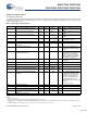
Table 33. 5V AC Operational Amplifier Specifications (continued)
Symbol Description Min Typ Max Unit
Table 34. 3.3V AC Operational Amplifier Specifications
Symbol Description Min Typ Max Units
T
ROA
Rising Settling Time from 80% of ΔV to 0.1% of ΔV (10 pF load, Unity Gain)
Power = Low, Opamp Bias = Low
Power = Low, Opamp Bias = High
–
–
–
–
3.92
0.72
μs
μs
T
SOA
Falling Settling Time from 20% of ΔV to 0.1% of ΔV (10 pF load, Unity Gain)
Power = Low, Opamp Bias = Low
Power = Medium, Opamp Bias = High
–
–
–
–
5.41
0.72
μs
μs
SR
ROA
Rising Slew Rate (20% to 80%)(10 pF load, Unity Gain)
Power = Low, Opamp Bias = Low
Power = Medium, Opamp Bias = High
0.31
2.7
–
–
–
–
V/μs
V/μs
SR
FOA
Falling Slew Rate (20% to 80%)(10 pF load, Unity Gain)
Power = Low, Opamp Bias = Low
Power = Medium, Opamp Bias = High
0.24
1.8
–
–
–
–
V/μs
V/μs
BW
OA
Gain Bandwidth Product
Power = Low, Opamp Bias = Low
Power = Medium, Opamp Bias = High
0.67
2.8
–
–
–
–
MHz
MHz
E
NOA
Noise at 1 kHz (Power = Medium, Opamp Bias = High) – 100 – nV/rt-Hz
100
1000
10000
0.001 0.01 0.1 1 10 100Freq (kHz)
dBV/rtHz
0
0.01
0.1
1.0
10
[+] Feedback