
User manual

CY8C27143, CY8C27243
CY8C27443, CY8C27543, CY8C27643
Document Number: 38-12012 Rev. *O Page 29 of 53
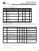
DC Analog PSoC Block Specifications
The following table lists guaranteed maximum and minimum specifications for the voltage and temperature ranges: 4.75V to 5.25V
and -40°C ≤ T
A
≤ 85°C, or 3.0V to 3.6V and -40°C ≤ T
A
≤ 85°C, respectively. Typical parameters apply to 5V and 3.3V at 25°C and
are for design guidance only.
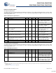
– RefLo = BandGap Not Allowed
– RefLo = 2 x BandGap - P2[6]
(P2[6] = 0.5V)
Not Allowed
– RefLo = P2[4] – BandGap
(P2[4] = Vdd/2)
Not Allowed
– RefLo = P2[4]-P2[6] (P2[4] = Vdd/2,
P2[6] = 0.5V)
P2[4] - P2[6] - 0.048 P2[4] - P2[6] + 0.022 P2[4] - P2[6] + 0.092 V
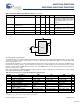
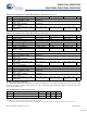
Table 26. Silicon Revision A – 3.3V DC Analog Reference Specifications (continued)
Symbol Description Min Typ Max Unit
Note
8. AGND tolerance includes the offsets of the local buffer in the PSoC block.
See Application Note AN2012 “Adjusting PSoC Microcontroller Trims for Dual Voltage-Range Operation” for information on trimming for operation at 3.3V.
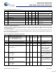
Table 27. Silicon Revision B – 3.3V DC Analog Reference Specifications
Symbol Description Min Typ Max Unit
BG Bandgap Voltage Reference 1.28 1.30 1.32 V
– AGND = Vdd/2
[8]
Vdd/2 - 0.027 Vdd/2 Vdd/2 + 0.005 V
– AGND = 2 x BandGap
[8]
Not Allowed
– AGND = P2[4] (P2[4] = Vdd/2) P2[4] - 0.008 P2[4] P2[4] + 0.009 V
– AGND = BandGap
[8]
BG - 0.009 BG BG + 0.009 V
– AGND = 1.6 x BandGap
[8]
1.6 x BG - 0.018 1.6 x BG 1.6 x BG + 0.018 V
– AGND Block to Block Variation
(AGND = Vdd/2)
[8]
-0.034 0.000 0.034 mV
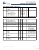
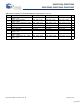
– RefHi = Vdd/2 + BandGap Not Allowed
– RefHi = 3 x BandGap Not Allowed
– RefHi = 2 x BandGap + P2[6]
(P2[6] = 0.5V)
Not Allowed
– RefHi = P2[4] + BandGap
(P2[4] = Vdd/2)
Not Allowed
– RefHi = P2[4] + P2[6] (P2[4] = Vdd/2,
P2[6] = 0.5V)
P2[4] + P2[6] - 0.06 P2[4] + P2[6] - 0.01 P2[4] + P2[6] + 0.057 V
– RefHi = 3.2 x BandGap Not Allowed
– RefLo = Vdd/2 - BandGap Not Allowed
– RefLo = BandGap Not Allowed
– RefLo = 2 x BandGap - P2[6]
(P2[6] = 0.5V)
Not Allowed
– RefLo = P2[4] – BandGap
(P2[4] = Vdd/2)
Not Allowed
– RefLo = P2[4]-P2[6] (P2[4] = Vdd/2,
P2[6] = 0.5V)
P2[4] - P2[6] - 0.048 P2[4] - P2[6] + 0.01 P2[4] - P2[6] + 0.048 V
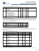
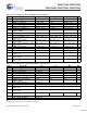
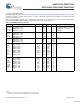
Table 28. DC Analog PSoC Block Specifications
Symbol Description Min Typ Max Unit
R
CT
Resistor Unit Value (Continuous Time) – 12.2 – kΩ
C
SC
Capacitor Unit Value (Switch Cap) – 80 – fF
[+] Feedback