
User manual

CY8C27143, CY8C27243
CY8C27443, CY8C27543, CY8C27643
Document Number: 38-12012 Rev. *O Page 28 of 53
Note
7.
AGND tolerance includes the offsets of the local buffer in the PSoC block.
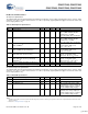
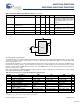
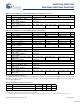
Table 25. Silicon Revision B – 5V DC Analog Reference Specifications
Symbol Description Min Typ Max Unit
BG Bandgap Voltage Reference 1.28 1.30 1.32 V
– AGND = Vdd/2
[7]
Vdd/2 - 0.030 Vdd/2 Vdd/2 + 0.007 V
– AGND = 2 x BandGap
[7]
2 x BG - 0.043 2 x BG 2 x BG + 0.024 V
– AGND = P2[4] (P2[4] = Vdd/2)
[7]
P2[4] - 0.011 P2[4] P2[4] + 0.011 V
– AGND = BandGap
[7]
BG - 0.009 BG BG + 0.009 V
– AGND = 1.6 x BandGap
[7]
1.6 x BG - 0.018 1.6 x BG 1.6 x BG + 0.018 V
– AGND Block to Block Variation
(AGND = Vdd/2)
[7]
-0.034 0.000 0.034 V
– RefHi = Vdd/2 + BandGap Vdd/2 + BG - 0.1 Vdd/2 + BG - 0.01 Vdd/2 + BG + 0.1 V
– RefHi = 3 x BandGap 3 x BG - 0.06 3 x BG - 0.01 3 x BG + 0.06 V
– RefHi = 2 x BandGap + P2[6]
(P2[6] = 1.3V)
2 x BG + P2[6] - 0.06 2 x BG + P2[6] - 0.01 2 x BG + P2[6] + 0.06 V
– RefHi = P2[4] + BandGap
(P2[4] = Vdd/2)
P2[4] + BG - 0.06 P2[4] + BG - 0.01 P2[4] + BG + 0.06 V
– RefHi = P2[4] + P2[6] (P2[4] = Vdd/2,
P2[6] = 1.3V)
P2[4] + P2[6] - 0.06 P2[4] + P2[6] - 0.01 P2[4] + P2[6] + 0.06 V
– RefHi = 3.2 x BandGap 3.2 x BG - 0.06 3.2 x BG - 0.01 3.2 x BG + 0.06 V
– RefLo = Vdd/2 – BandGap Vdd/2 - BG - 0.051 Vdd/2 - BG
+
0.01 Vdd/2 - BG + 0.06 V
– RefLo = BandGap BG - 0.06 BG + 0.01 BG + 0.06 V
– RefLo = 2 x BandGap - P2[6]
(P2[6] = 1.3V)
2 x BG - P2[6] - 0.04 2 x BG - P2[6] + 0.01 2 x BG - P2[6] + 0.04 V
– RefLo = P2[4] – BandGap
(P2[4] = Vdd/2)
P2[4] - BG - 0.056 P2[4] - BG + 0.01 P2[4] - BG + 0.056 V
– RefLo = P2[4]-P2[6] (P2[4] = Vdd/2,
P2[6] = 1.3V)
P2[4] - P2[6] - 0.056 P2[4] - P2[6] + 0.01 P2[4] - P2[6] + 0.056 V
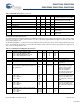
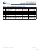
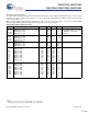
Table 26. Silicon Revision A – 3.3V DC Analog Reference Specifications
Symbol Description Min Typ Max Unit
BG Bandgap Voltage Reference 1.274 1.30 1.326 V
– AGND = Vdd/2
[8]
Vdd/2 - 0.027 Vdd/2 - 0.003 Vdd/2 + 0.002 V
– AGND = 2 x BandGap
[8]
Not Allowed
– AGND = P2[4] (P2[4] = Vdd/2) P2[4] - 0.008 P2[4] + 0.001 P2[4] + 0.009 V
– AGND = BandGap
[8]
BG - 0.009 BG BG + 0.009 V
– AGND = 1.6 x BandGap
[8]
1.6 x BG - 0.018 1.6 x BG 1.6 x BG + 0.018 V
– AGND Block to Block Variation
(AGND = Vdd/2)
[8]
-0.034 0.000 0.034 V
– RefHi = Vdd/2 + BandGap Not Allowed
– RefHi = 3 x BandGap Not Allowed
– RefHi = 2 x BandGap + P2[6]
(P2[6] = 0.5V)
Not Allowed
– RefHi = P2[4] + BandGap
(P2[4] = Vdd/2)
Not Allowed
– RefHi = P2[4] + P2[6] (P2[4] = Vdd/2,
P2[6] = 0.5V)
P2[4] + P2[6] - 0.075 P2[4] + P2[6] - 0.009 P2[4] + P2[6] + 0.057 V
– RefHi = 3.2 x BandGap Not Allowed
– RefLo = Vdd/2 - BandGap Not Allowed
[+] Feedback