
User manual

CY8C27143, CY8C27243
CY8C27443, CY8C27543, CY8C27643
Document Number: 38-12012 Rev. *O Page 26 of 53
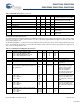
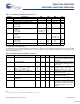
Figure 11. Basic Switch Mode Pump Circuit
DC Analog Reference Specifications
The following tables list guaranteed maximum and minimum specifications for the voltage and temperature ranges: 4.75V to 5.25V
and -40°C ≤ T
A
≤ 85°C, or 3.0V to 3.6V and -40°C ≤ T
A
≤ 85°C, respectively. Typical parameters apply to 5V and 3.3V at 25°C and
are for design guidance only.
The guaranteed specifications are measured through the Analog Continuous Time PSoC blocks. The power levels for AGND refer to
the power of the Analog Continuous Time PSoC block. The power levels for RefHi and RefLo refer to the Analog Reference Control
register. The limits stated for AGND include the offset error of the AGND buffer local to the Analog Continuous Time PSoC block.
Reference control power is high.
Note Avoid using P2[4] for digital signaling when using an analog resource that depends on the Analog Reference. Some coupling
of the digital signal may appear on the AGND.
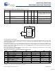
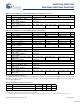
ΔV
PUMP_Load
Load Regulation – 5 – %V
O
Configuration of footnote.
[5]
V
O
is the
“Vdd Value for PUMP Trip” specified
by the VM[2:0] setting in the DC POR
and LVD Specification, Table 29 on
page 30.
ΔV
PUMP_Ripple
Output Voltage Ripple (depends on
capacitor/load)
– 100 – mVpp Configuration of footnote.
[5]
Load is 5
mA.
E
3
Efficiency 35 50 – % Configuration of footnote.
[5]
Load is 5
mA. SMP trip voltage is set to 3.25V.
F
PUMP
Switching Frequency – 1.3 – MHz
DC
PUMP
Switching Duty Cycle – 50 – %
Table 23. DC Switch Mode Pump (SMP) Specifications (continued)
Symbol Description Min Typ Max Unit Notes
Battery
C1
D1
+
PSoC
TM
Vdd
Vss
SMP
V
BAT
V
PUMP
L
1
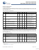
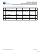
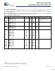
Table 24. Silicon Revision A – 5V DC Analog Reference Specifications
Symbol Description Min Typ Max Unit
BG Bandgap Voltage Reference 1.274 1.30 1.326 V
– AGND = Vdd/2
[6]
Vdd/2 - 0.030 Vdd/2 - 0.004 Vdd/2 + 0.003 V
– AGND = 2 x BandGap
[6]
2 x BG - 0.043 2 x BG - 0.010 2 x BG + 0.024 V
– AGND = P2[4] (P2[4] = Vdd/2)
[6]
P2[4] - 0.013 P2[4] P2[4] + 0.014 V
– AGND = BandGap
[6]
BG - 0.009 BG BG + 0.009 V
– AGND = 1.6 x BandGap
[6]
1.6 x BG - 0.018 1.6 x BG 1.6 x BG + 0.018 V
– AGND Block to Block Variation
(AGND = Vdd/2)
[6]
-0.034 0.000 0.034 V
– RefHi = Vdd/2 + BandGap Vdd/2 + BG - 0.140 Vdd/2 + BG - 0.018 Vd
d
/2 + BG + 0.103 V
– RefHi = 3 x BandGap 3 x BG - 0.112 3 x BG - 0.018 3 x BG + 0.076 V
Note
6. AGND tolerance includes the offsets of the local buffer in the PSoC block.
[+] Feedback