
User manual

CY8C27143, CY8C27243
CY8C27443, CY8C27543, CY8C27643
Document Number: 38-12012 Rev. *O Page 24 of 53
DC Low Power Comparator Specifications
The following table lists guaranteed maximum and minimum specifications for the voltage and temperature ranges: 4.75V to 5.25V
and -40°C ≤ T
A
≤ 85°C, 3.0V to 3.6V and -40°C ≤ T
A
≤ 85°C, or 2.4V to 3.0V and -40°C ≤ T
A
≤ 85°C, respectively. Typical parameters
apply to 5V at 25°C and are for design guidance only.
DC Analog Output Buffer Specifications
The following tables list guaranteed maximum and minimum specifications for the voltage and temperature ranges: 4.75V to 5.25V
and -40°C ≤ T
A
≤ 85°C, or 3.0V to 3.6V and -40°C ≤ T
A
≤ 85°C, respectively. Typical parameters apply to 5V and 3.3V at 25°C and
are for design guidance only.
V
OLOWOA
Low Output Voltage Swing (internal signals)
Power = Low
Power = Medium
Power = High
–
–
–
–
–
–
0.2
0.2
0.2
V
V
V
I
SOA
Supply Current (including associated AGND
buffer)
Power = Low, Opamp Bias = Low
Power = Low, Opamp Bias = High
Power = Medium, Opamp Bias = Low
Power = Medium, Opamp Bias = High
Power = High, Opamp Bias = Low
Power = High, Opamp Bias = High
–
–
–
–
–
–
150
300
600
1200
2400
4600
200
400
800
1600
3200
6400
μA
μA
μA
μA
μA
μA
PSRR
OA
Supply Voltage Rejection Ratio 50 80 – dB Vss ≤ VIN ≤ (Vdd - 2.25) or
(Vdd - 1.25V) ≤ VIN ≤ Vdd.
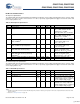
Table 19. 3.3V DC Operational Amplifier Specifications (continued)
Symbol Description Min Typ Max Unit Notes
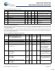
Table 20. DC Low Power Comparator Specifications
Symbol Description Min Typ Max Unit
V
REFLPC
Low power comparator (LPC) reference
voltage range
0.2 – Vdd - 1 V
I
SLPC
LPC supply current – 10 40 μA
V
OSLPC
LPC voltage offset – 2.5 30 mV
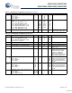
Table 21. 5V DC Analog Output Buffer Specifications
Symbol Description Min Typ Max Unit
V
OSOB
Input Offset Voltage (Absolute Value) – 3 12 mV
TCV
OSOB
Average Input Offset Voltage Drift – +6 – μV/°C
V
CMOB
Common-Mode Input Voltage Range 0.5 – Vdd - 1.0 V
R
OUTOB
Output Resistance
Power = Low
Power = High
–
–
1
1
–
–
W
W
V
OHIGHOB
High Output Voltage Swing (Load = 32 ohms
to Vdd/2)
Power = Low
Power = High
0.5 x Vdd
+ 1.3
0.5 x Vdd
+ 1.3
–
–
–
–
V
V
V
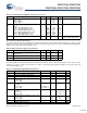
OLOWOB
Low Output Voltage Swing (Load = 32 ohms
to Vdd/2)
Power = Low
Power = High
–
–
–
–
0.5 x Vdd
- 1.3
0.5 x Vdd
- 1.3
V
V
I
SOB
Supply Current Including Bias Cell (No Load)
Power = Low
Power = High
–
–
1.1
2.6
5.1
8.8
mA
mA
PSRR
OB
Supply Voltage Rejection Ratio 60 64 – dB
I
OMAX
Maximum Output Current – 40 – mA
[+] Feedback