
User manual

CY8C27143, CY8C27243
CY8C27443, CY8C27543, CY8C27643
Document Number: 38-12012 Rev. *O Page 21 of 53
DC Electrical Characteristics
DC Chip-Level Specifications
The following table lists guaranteed maximum and minimum specifications for the voltage and temperature ranges: 4.75V to 5.25V
and -40°C ≤ T
A
≤ 85°C, or 3.0V to 3.6V and -40°C ≤ T
A
≤ 85°C, respectively. Typical parameters apply to 5V and 3.3V at 25°C and
are for design guidance only.
DC General Purpose I/O Specifications
The following table lists guaranteed maximum and minimum specifications for the voltage and temperature ranges: 4.75V to 5.25V
and -40°C ≤ T
A
≤ 85°C, or 3.0V to 3.6V and -40°C ≤ T
A
≤ 85°C, respectively. Typical parameters apply to 5V and 3.3V at 25°C and
are for design guidance only.
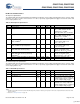
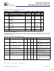
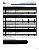
Table 16. DC Chip-Level Specifications
Symbol Description Min Typ Max Unit Notes
Vdd Supply Voltage 3.00 – 5.25 V
I
DD
Supply Current – 5 8 mA Conditions are Vdd = 5.0V, T
A
= 25
o
C,
CPU = 3 MHz, SYSCLK doubler
disabled. VC1 = 1.5 MHz,
VC2 = 93.75 kHz, VC3 = 93.75 kHz.
I
DD3
Supply Current – 3.3 6.0 mA Conditions are Vdd = 3.3V, T
A
= 25
o
C,
CPU = 3 MHz, SYSCLK doubler
disabled. VC1 = 1.5 MHz,
VC2 = 93.75 kHz, VC3 = 93.75 kHz.
I
SB
Sleep (Mode) Current with POR, LVD, Sleep
Timer, and WDT.
[3]
– 3 6.5 μA Conditions are with internal slow
speed oscillator, Vdd = 3.3V,
-40
o
C ≤ T
A
≤ 55
o
C.
I
SBH
Sleep (Mode) Current with POR, LVD, Sleep
Timer, and WDT at high temperature.
[3]
– 4 25 μA Conditions are with internal slow
speed oscillator, Vdd = 3.3V,
55
o
C < T
A
≤ 85
o
C.
I
SBXTL
Sleep (Mode) Current with POR, LVD, Sleep
Timer, WDT, and external crystal.
[3]
– 4 7.5 μA Conditions are with properly loaded, 1
μW max, 32.768 kHz crystal.
Vdd = 3.3V, -40
o
C ≤ T
A
≤ 55
o
C.
I
SBXTLH
Sleep (Mode) Current with POR, LVD, Sleep
Timer, WDT, and external crystal at high
temperature.
[3]
– 5 26 μA Conditions are with properly loaded, 1
μW max, 32.768 kHz crystal.
Vdd = 3.3V, 55
o
C < T
A
≤ 85
o
C.
V
REF
Reference Voltage (Bandgap) for Silicon A
[4]
1.275 1.300 1.325 V Trimmed for appropriate Vdd.
V
REF
Reference Voltage (Bandgap) for Silicon B
[4]
1.280 1.300 1.320 V Trimmed for appropriate Vdd.
Notes
3. Standby current includes all functions (POR, LVD, WDT, Sleep Time) needed for reliable system operation. This must be compared with devices that have similar
functions enabled.
4. Refer to the “Ordering Information” on page 50.
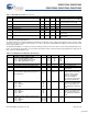
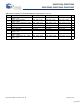
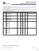
Table 17. DC GPIO Specifications
Symbol Description Min Typ Max Unit Notes
R
PU
Pull up Resistor 4 5.6 8 kΩ
R
PD
Pull down Resistor 4 5.6 8 kΩ
V
OH
High Output Level Vdd -
1.0
– – V IOH = 10 mA, Vdd = 4.75 to 5.25V
(8 total loads, 4 on even port pins (for
example, P0[2], P1[4]), 4 on odd port
pins (for example, P0[3], P1[5])).
V
OL
Low Output Level – – 0.75 V IOL = 25 mA, Vdd = 4.75 to 5.25V (8
total loads, 4 on even port pins (for
example, P0[2], P1[4]), 4 on odd port
pins (for example, P0[3], P1[5])).
[+] Feedback