
User manual

CY8C27143, CY8C27243
CY8C27443, CY8C27543, CY8C27643
Document Number: 38-12012 Rev. *O Page 16 of 53
Register Reference
This chapter lists the registers of the CY8C27x43 PSoC device.
For detailed register information, reference the
PSoC Programmable System-on-Chip Technical Reference
Manual.
Register Conventions
The register conventions specific to this section are listed in the
following table.
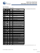
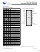
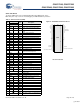
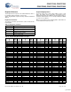
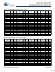
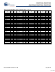
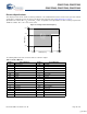
Register Mapping Tables
The PSoC device has a total register address space of 512
bytes. The register space is referred to as I/O space and is
divided into two banks. The XOI bit in the Flag register (CPU_F)
determines which bank the user is currently in. When the XOI bit
is set the user is in Bank 1.
Note In the following register mapping tables, blank fields are
reserved and must not be accessed.
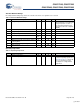
Table 10. Register Conventions
Convention Description
R Read register or bit(s)
W Write register or bit(s)
L Logical register or bit(s)
C Clearable register or bit(s)
# Access is bit specific
Table 11. Register Map Bank 0 Table: User Space
Name
Addr
(0,Hex)
Access
Name
Addr
(0,Hex)
Access
Name
Addr
(0,Hex)
Access
Name
Addr
(0,Hex)
Access
PRT0DR 00 RW 40 ASC10CR0 80 RW C0
PRT0IE 01 RW 41 ASC10CR1 81 RW C1
PRT0GS 02 RW 42 ASC10CR2 82 RW C2
PRT0DM2 03 RW 43 ASC10CR3 83 RW C3
PRT1DR 04 RW 44 ASD11CR0 84 RW C4
PRT1IE 05 RW 45 ASD11CR1 85 RW C5
PRT1GS 06 RW 46 ASD11CR2 86 RW C6
PRT1DM2 07 RW 47 ASD11CR3 87 RW C7
PRT2DR 08 RW 48 ASC12CR0 88 RW C8
PRT2IE 09 RW 49 ASC12CR1 89 RW C9
PRT2GS 0A RW 4A ASC12CR2 8A RW CA
PRT2DM2 0B RW 4B ASC12CR3 8B RW CB
PRT3DR 0C RW 4C ASD13CR0 8C RW CC
PRT3IE 0D RW 4D ASD13CR1 8D RW CD
PRT3GS 0E RW 4E ASD13CR2 8E RW CE
PRT3DM2 0F RW 4F ASD13CR3 8F RW CF
PRT4DR 10 RW 50 ASD20CR0 90 RW D0
PRT4IE 11 RW 51 ASD20CR1 91 RW D1
PRT4GS 12 RW 52 ASD20CR2 92 RW D2
PRT4DM2 13 RW 53 ASD20CR3 93 RW D3
PRT5DR 14 RW 54 ASC21CR0 94 RW D4
PRT5IE 15 RW 55 ASC21CR1 95 RW D5
PRT5GS 16 RW 56 ASC21CR2 96 RW I2C_CFG D6 RW
PRT5DM2 17 RW 57 ASC21CR3 97 RW I2C_SCR D7 #
18 58 ASD22CR0 98 RW I2C_DR D8 RW
19 59 ASD22CR1 99 RW I2C_MSCR D9 #
1A 5A ASD22CR2 9A RW INT_CLR0 DA RW
1B 5B ASD22CR3 9B RW INT_CLR1 DB RW
1C 5C ASC23CR0 9C RW DC
1D 5D ASC23CR1 9D RW INT_CLR3 DD RW
1E 5E ASC23CR2 9E RW INT_MSK3 DE RW
1F 5F ASC23CR3 9F RW DF
DBB00DR0 20 # AMX_IN 60 RW A0 INT_MSK0 E0 RW
DBB00DR1 21 W 61 A1 INT_MSK1 E1 RW
DBB00DR2 22 RW 62 A2 INT_VC E2 RC
DBB00CR0 23 # ARF_CR 63 RW A3 RES_WDT E3 W
DBB01DR0 24 # CMP_CR0 64 # A4 DEC_DH E4 RC
DBB01DR1 25 W ASY_CR 65 # A5 DEC_DL E5 RC
Blank fields are Reserved and must not be accessed. # Access is bit specific.
[+] Feedback