
User manual

CY8C27143, CY8C27243
CY8C27443, CY8C27543, CY8C27643
Document Number: 38-12012 Rev. *O Page 15 of 53
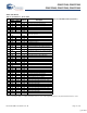
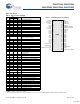
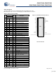
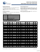
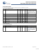
42 OCD HCLK OCD high-speed clock output.
43 OCD CCLK OCD CPU clock output.
44 I/O P4[0]
45 I/O P4[2]
46 I/O P4[4]
47 I/O P4[6]
48 I/O I P2[0] Direct switched capacitor block input.
49 I/O I P2[2] Direct switched capacitor block input.
50 I/O P2[4] External Analog Ground (AGND).
51 I/O P2[6] External Voltage Reference (VRef).
52 I/O I P0[0] Analog column mux input.
53 I/O I P0[2] Analog column mux input and column
output.
54 I/O I P0[4] Analog column mux input and column
output.
55 I/O I P0[6] Analog column mux input.
56 Power Vdd Supply voltage.
LEGEND: A = Analog, I = Input, O = Output, and OCD = On-Chip Debug.
* These are the ISSP pins, which are not High Z at POR (Power On Reset). See the PSoC Mixed-Signal Array Technical Reference Manual for details.
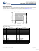
Table 9. 56-Pin Part Pinout (SSOP)
[+] Feedback