
User manual

CY8C27143, CY8C27243
CY8C27443, CY8C27543, CY8C27643
Document Number: 38-12012 Rev. *O Page 11 of 53
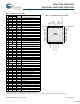
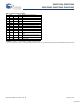
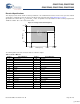
44-Pin Part Pinout
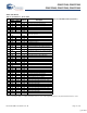
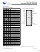
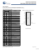
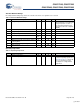
Table 6. Pin Definitions - 44-Pin TQFP
Pin
No.
Type
Pin Name Description
Figure 6. CY8C27543 44-Pin PSoC Device
Digital Analog
1 I/O P2[5]
2 I/O I P2[3] Direct switched capacitor block input.
3 I/O I P2[1] Direct switched capacitor block input.
4 I/O P4[7]
5 I/O P4[5]
6 I/O P4[3]
7 I/O P4[1]
8 Power SMP Switch Mode Pump (SMP) connection to external
components required.
9 I/O P3[7]
10 I/O P3[5]
11 I/O P3[3]
12 I/O P3[1]
13 I/O P1[7] I2C Serial Clock (SCL).
14 I/O P1[5] I2C Serial Data (SDA).
15 I/O P1[3]
16 I/O P1[1] Crystal Input (XTALin), I2C Serial Clock (SCL),
ISSP-SCLK*.
17 Power Vss Ground connection.
18 I/O P1[0] Crystal Output (XTALout), I2C Serial Data (SDA),
ISSP-SDATA*.
19 I/O P1[2]
20 I/O P1[4] Optional External Clock Input (EXTCLK).
21 I/O P1[6]
22 I/O P3[0]
23 I/O P3[2]
24 I/O P3[4]
25 I/O P3[6]
26 Input XRES Active high external reset with internal pull down.
27 I/O P4[0]
28 I/O P4[2]
29 I/O P4[4]
30 I/O P4[6]
31 I/O I P2[0] Direct switched capacitor block input.
32 I/O I P2[2] Direct switched capacitor block input.
33 I/O P2[4] External Analog Ground (AGND).
34 I/O P2[6] External Voltage Reference (VRef).
35 I/O I P0[0] Analog column mux input.
36 I/O I/O P0[2] Analog column mux input and column output.
37 I/O I/O P0[4] Analog column mux input and column output.
38 I/O I P0[6] Analog column mux input.
39 Power Vdd Supply voltage.
40 I/O I P0[7] Analog column mux input.
41 I/O I/O P0[5] Analog column mux input and column output.
42 I/O I/O P0[3] Analog column mux input and column output.
43 I/O I P0[1] Analog column mux input.
44 I/O P2[7]
LEGEND: A = Analog, I = Input, and O = Output.
* These are the ISSP pins, which are not High Z at POR (Power On Reset). See the PSoC Programmable System-on-Chip Technical Reference Manual for details.
[+] Feedback